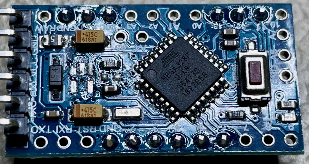
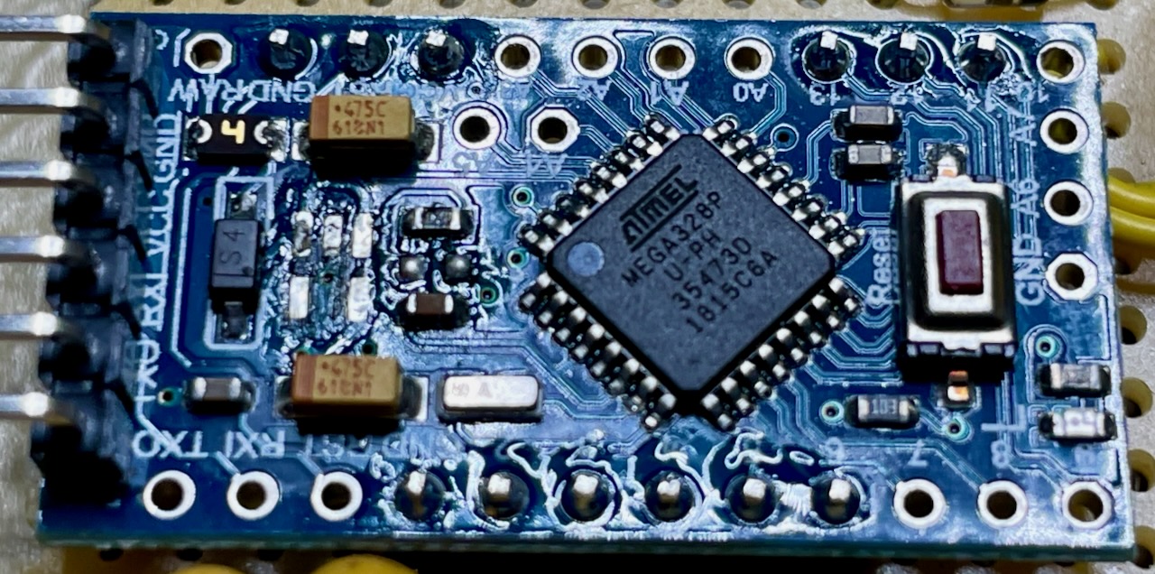
The Pro Mini had its power Led and regulator removed and was flashed with the standard Arduino boot loader as well as fuse settings.
With all I/O pins turned off and microcontroller put to SLEEP_MODE_IDLE, waking up once every millisecond to service the millis() timer and run once through the program main loop, the power consumption turned out to be around 5 mA.
This is a surprisingly low power consumption, considering that the Pro Mini would usually draw around 10 mA under the same operating conditions.
I have ran the exact same firmware on a different Pro Mini specimen (after accidentally damaging the original one), which ended up drawing the expected ~10 mA.
Following my observations, I have went for the quest of finding out the root cause of this power consumption discrepancy of seemingly identical Arduino Pro Minis.
I have double checked the fuses settings and made sure that both Pro Minis run the exact same bootloader version, which they did.
By the way, the following commands have been used for reading the fuse settings on Mac OS with Arduino IDE 1.8.19 using the “Arduino as ISP” programmer:
It turns out that there are “fake” ATmega328P versions that are difficult to distinguish from the original ones. These fake units fully compatible with the original, except for having different power consumption characteristics.
According to the above sources, the fake units have a much higher SLEEP_MODE_PWR_DOWN mode current consumption of ~150 µA, as compared to less than 1 µA for the original units. However, according to my observation described above, these fake units seem to draw 50% less current in SLEEP_MODE_IDLE (~5 mA vs ~10 mA).
Furthermore, it is possible to distinguish fake units from their genuine counterparts by loading the following sketch:
// Found this code here
// https://gist.github.com/speters/f889faec42b510052a6ab4be437d38ca
// Purpose is to simply run a memory check on ATMEGA238P to test for counterfeit parts

#include <avr/boot.h>
#define SIGRD 5

void setup() {
  // put your setup code here, to run once:
  Serial.begin(115200);
  Serial.println("");
  Serial.println("boot sig dump");
  int newLineIndex = 0;
  for (uint8_t i = 0; i <= 0x1F; i += 1) {
    Serial.print(boot_signature_byte_get(i), HEX);
    Serial.print("\t");
    newLineIndex++;
    if (newLineIndex == 8) {
      Serial.println("");
      newLineIndex = 0;
    }
  }
  Serial.println();
}

void loop() {
}
The genuine units will generate a boot signature similar to:
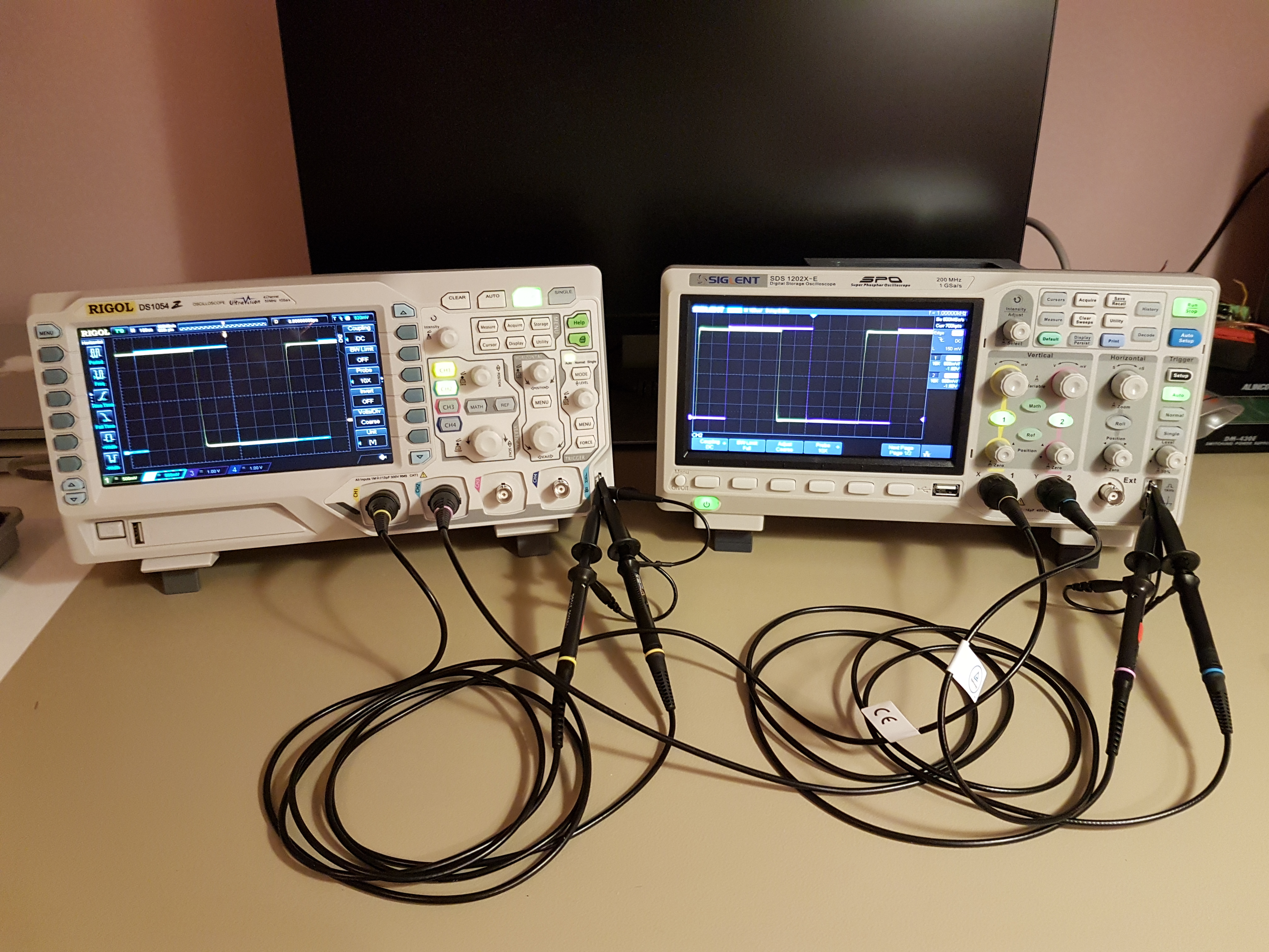
This article describes a method for the very precise measurement of a frequency difference using an oscilloscope with multiple channels.
The following video shows the display of an oscilloscope whose four channels are connected to four different Temperature Compensated Crystal Oscillators (TCXOs).
As seen in the above video, four different waveforms originating form the oscillators are displayed on the oscilloscope screen. The TCXOs are very accurate and are rated at , so their frequencies are very close to each other. The waveform on channel 4 (dark blue) has been used as the trigger source, this waveform shall represent the reference frequency . The waveforms on channels 1, 2 and 3 (yellow, light blue and purple) are slowly drifting relative to the reference waveform. Thus, these waveforms have ever so slightly different frequencies whose difference we are about to determine.
In order to determine the exact frequency difference , we need to first measure how fast the corresponding waveform is scrolling relative to the reference waveform. For this purpose, we shall define as the time duration in seconds that is required for the waveform to move by one whole period relative to one of the fixed vertical lines on the oscilloscope screen. can be determined by visually observing the waveform and measuring one period scroll duration using a stopwatch.
If a waveform is scrolling towards the left side relative to the reference waveform, then its frequency is larger than and shall have a positive sign. The opposite is true if the waveform is scrolling towards the right side, then its frequency is smaller than and shall have a negative sign.
Whenever elapses, the measured waveform will advance or retard by one full period duration relative to the reference waveform.
For , the measured waveform will advance by exactly one period per second. Consequently, the frequency difference relative to would be . This behaviour can be generalised by the following formula:
The difference in parts per million can be calculated as follows:
The TCXOs measured in the above setup have been used for increasing the accuracy of a classic Casio digital wrist watch. Hence, it is of our interest to calculate the particular oscillator’s drift in seconds per day. This can be done using the following formula:
Taking the purple waveform on channel 3 as an example, we can measure . This would yield to .
For the above example, and .
I hope that you found this article useful. Please be welcome post your feedback and comments below.
The following article explains the theory of operation of an ideal diode circuit implemented using a p-channel MOSFET and a matched PNP transistor pair. Typical applications for the ideal diode are devices such as solar chargers, where power efficiency is of a great importance.
Table of Contents
Introduction
Diodes are devices that allow the electric current to flow in only one direction. As shown in the image below, the current is allowed to flow from the anode towards the cathode but not the other way around.
Diodes have many applications ranging from simple reverse polarity protection to full bridge rectifiers. There is plenty of available material explaining the diode basics, therefore I would like to skip this part and only cover one particular aspect of diodes which makes them rather power inefficient devices. This article shall cover the forward voltage drop denoted in the datasheet as .
is the voltage measured between the anode and the cathode of a diode subjected to an electric current in its forward direction. Whereas the anode corresponds to the positive side and the cathode to the negative. Typical values of are 0.6 Volts for a standard silicone Diode and as low as 0.1 Volts for a Schottky type diode. The value of is a function of the forward bias current as shown in the diagram below.
The above diagram plots the forward voltage drop (horizontal axis) versus the forward bias current (vertical axis) for a 1N4007 or similar diode. As one can see, can go as high as 1 Volt for 1 Ampere of current, which results in a dissipated power loss of 1 Watt.
As the name of this article suggests, the ideal diode is one which exhibits no (or very little) power loss. Thus, it should have (or close to) for a wide range of . Presented in this article is a small circuit that mimics the behavior of of a diode with a near zero forward voltage drop.
Circuit Diagram
As seen in the schematic below, the ideal diode consists of a p-channel MOSFET Q2 and a voltage comparator consisting of a matched PNP transistor pair Q1A and Q1B.
MOSFET
The IRLML2244 p-channel MOSFET Q2 is driven in the reverse direction, whereas its drain pin 3 is connected to the input voltage and its source pin 2 provides the output voltage . This ensures that the MOSFET’s intrinsic diode is aligned in the direction of forward current flow and prevents any reverse current from flowing through it.
This MOSFET exhibits a very low static drain-to-source on-resistance at a gate-source voltage of and a drain current of (see datasheet). The resulting measured forward voltage drop amounts to at .
Voltage Comparator
A voltage comparator circuit has been implemented around the PNP transistors Q1A and Q1B. It is important that these transistors have identical characteristics, otherwise the comparator will not have the required precision. Thus, these transistors part of a BC857BS matched transistor pair sharing the same package. Having both transistors inside one physical package ensures that they are thermally coupled and avoids diverging characteristics due to different junction temperatures.
The voltage comparator compares the voltages to and controls the MOSFET gate voltage across the resistor R2.
The following equations apply for the voltage between the transistor’s base and the power supply ground:
where and are the emitter-base voltages of transistors Q1A and Q1B. And:
Where is the specified base-emitter voltage drop for BC857BS (see datasheet). Due to the properties of the base-emitter junction which is essentially a diode, the voltages and are clamped to . A current can only flow through the emitter-base junction of Q1A or Q1B if the corresponding emitter-base voltage or reaches (gets slightly higher than) .
Forward Bias
The following holds true when the ideal diode is forward biased:
The larger of and will be clamped to which leads to the following statements:
Consequently, current will flow through the emitter-collector path of transistor Q1A while no current will flow through the emitter-collector path of Q1B. Thus, the voltage across the resistor R2 will be equal (or near equal) to 0V. This will lead to a negative gate-source voltage and cause the MOSFET Q1B to turn on.
Reverse Bias
The following holds true when the ideal diode is reverse biased:
The larger of and will be clamped to which leads to the following statements:
Consequently, current will flow through the emitter-collector path of transistor Q1B while no current will flow through the emitter-collector path of Q1A. Thus, the voltage across the resistor R2 will be equal (or near equal) to . This will lead to near zero gate-source voltage and cause the MOSFET Q1B to turn off.
PCB Layout
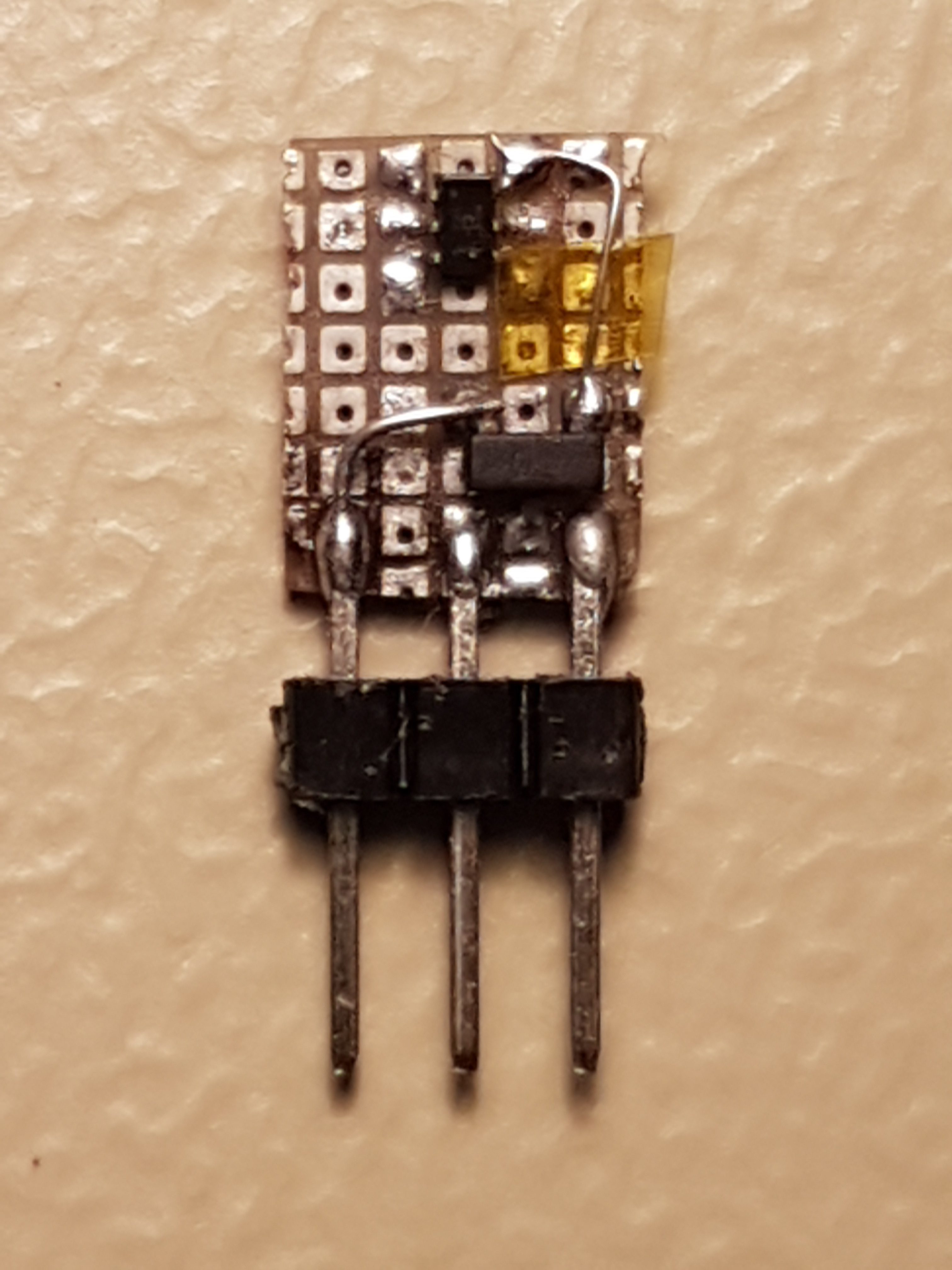
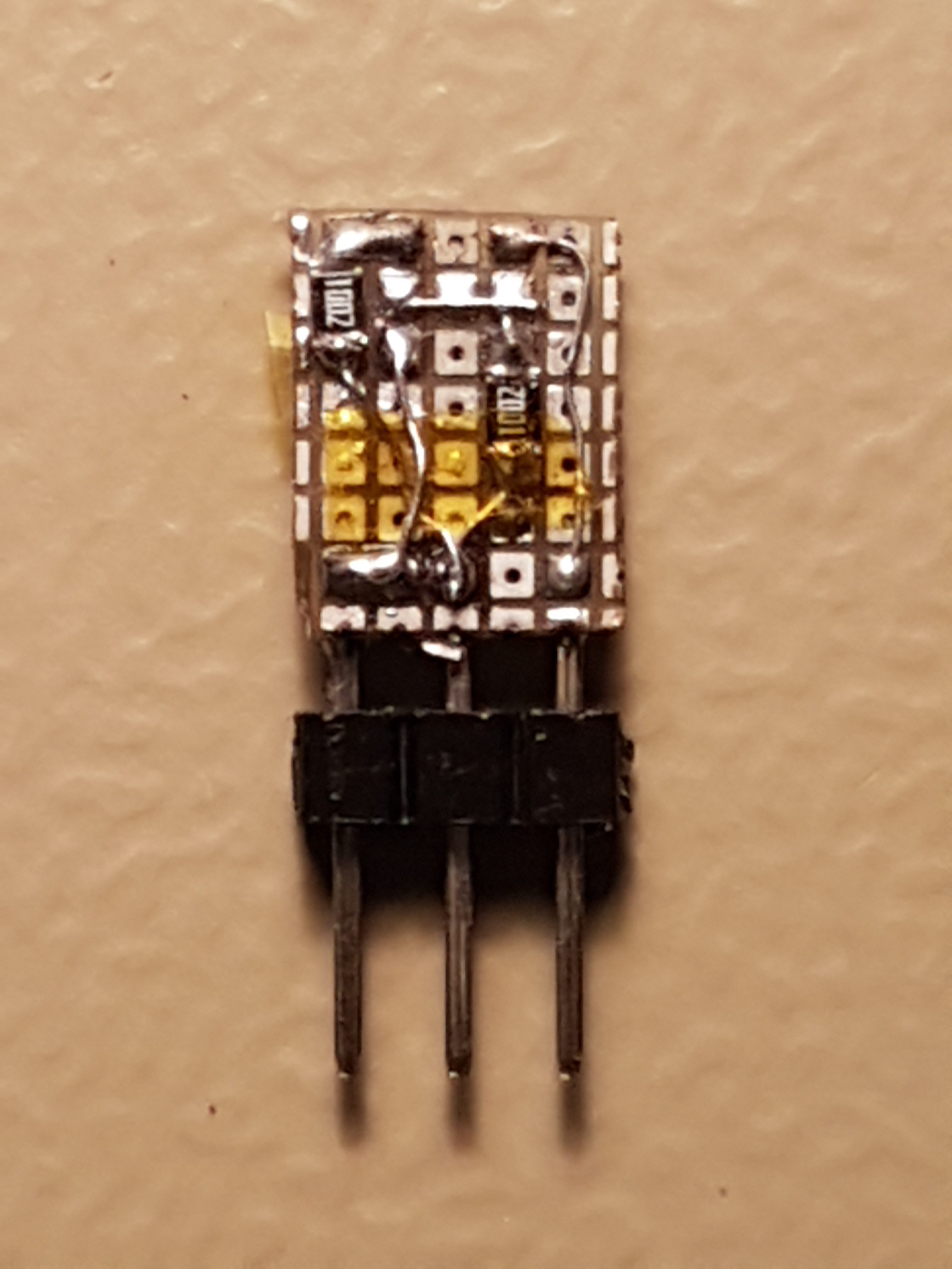
The circuit has been implemented on a SMD prototyping board as shown in the pictures below. The surface mount MOSFET, transistor pair and 0805 resistors have been connected using jumper wires. The three terminals of the ideal diode have been connected to a pin header.
The left picture shows the top side of the PCB with the visible MOSFET (3 pin package) and dual transistor (6 pin package). The right picture shows the backside of the PCB with the two 0805 resistors. Note that the pads on both sides are connected through the holes.
Following are the pin assignments on the pin header, assuming pin 1 is the leftmost pin and pin 3 is the rightmost pin on the left picture:
Pin 1:
Pin 2: GND
Pin 3:
Bill of Material
Following is the list of parts required for building the ideal diode. Please consider supporting this website by purchasing your the required parts using the affiliate links below:
IRLML2244 logic level p-channel MOSFET
BC857BS PNP transistor pair
10KΩ 0805 SMD resistors
2.54mm pin header
SMD prototyping board
Update (April 19, 2021)
David Albert has kindly provided the following feedback to this design. With his permission, I hereby quote his emails and diagrams he has provided.
Feedback on April 14, 2021
Hi Karim,
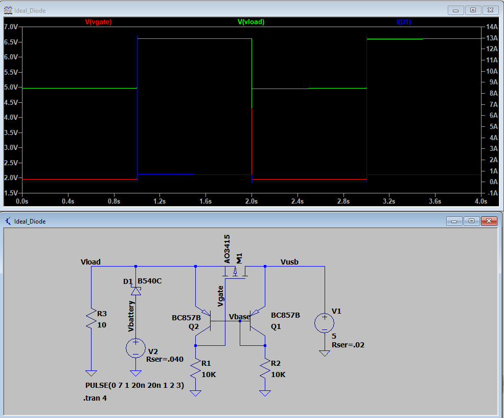
I found your ideal diode circuit on your blog (https://www.microfarad.de/blog/the-ideal-diode/); thanks for sharing it; it’s a clever design! I simulated it in LTSpice and it appeared to work, so I designed it into a circuit as an ideal diode replacement for ORing USB power with a 6-7V battery.
Unfortunately, I found that whenever I connected the battery, the USB port experienced a surge and would shut down. I went back to the simulation and I think I see the problem; if you agree, I think it would be good to note it on your blog so others don’t have the same problem. I’m still thinking about how to fix it and will let you know if I come up with an elegant solution (please let me know if you come up with one too).
The problem is that the MOSFET requires a finite amount of time to turn off. When the battery (V2 in my circuit) turns on, the BE junction of Q2 is forward biased and current flows through it and R2, causing a larger current flow through the emitter to collector (as your circuit intends); this works as designed. This current through Q2 is what charges M1’s gate causing it to turn off. Unfortunately, the BC857BS has a maximum current of 200mA and that charges the MOSFET gate slowly (high-current MOSFET drivers exist for exactly this reason: to charge/discharge gate capacitance quickly).
During the time Q2 is charging M1’s gate, M1 remains on and creates a short circuit between the two power sources and a *lot* of current will flow. This caused the protection circuitry on my USB port to kick in and shut down the port, but it could do much worse if such protection circuitry is not present.
The LTSpice simulation actually shows this problem (I just wasn’t sharp enough to look for it when I simulated it initially). The blue trace below shows the current through D1 (output of battery). Notice how the current surges momentarily above 13A. You can reduce the size of the surge (and the power consumption of the circuit) by increasing R1. You can reduce the surge a little more (at the expense of wasted power) by reducing R2, but the underlying problem remains: there is a brief period when the supplies are short circuited.
I’ve attached the LTSpice simulation in case you want to try it yourself…if you have any ideas for an elegant fix, I’d be grateful if you’d share them.
Thanks and regards, Dave Albert
Follow-up on April 14, 2021
Hi Karim,
You are welcome to post the explanation and thank you for looking at it and responding so quickly!
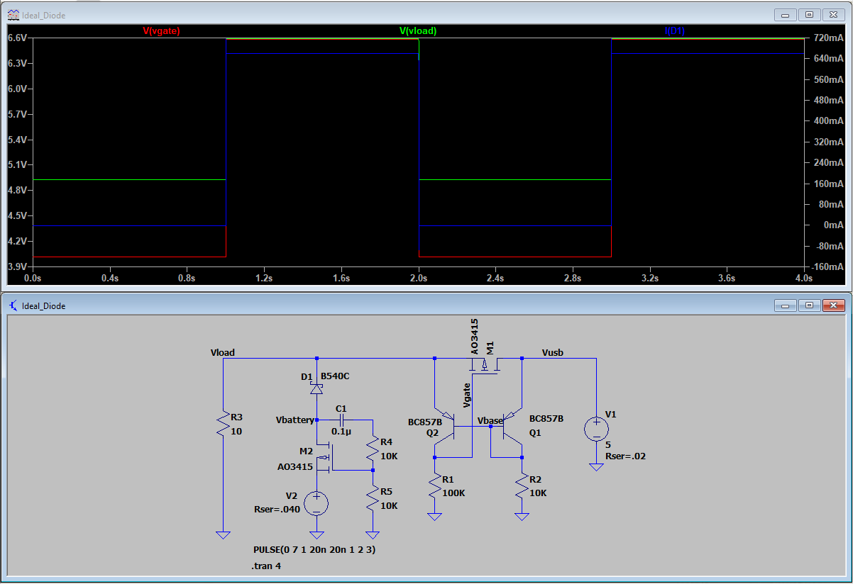
I slept on it and adding a soft-start circuit to the higher voltage source seems likely to solve the issue (and is probably a good idea anyway to reduce capacitor inrush currents). I simulated it below; the values shown below were not carefully chosen; I’ll tweak them later and then test it, but the simulation seems to work without the large reverse currents. If you have any better ideas, please let me know.
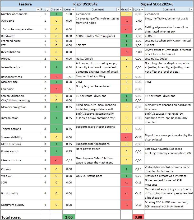
I’ve been lately searching for an entry level digital sampling oscilloscope (DSO) around the 400€ price tag. Having exhaustively read through the various forums and watched the numerous product reviews on YouTube, it became pretty clear that there are currently two major candidates on the market that fulfil the current price tag and provide a decent feature set.
Rigol DS1054Z
Siglent SDS1202X-E
Most of the product reviews that I have come across were clearly biased towards the one or the other device. Thus, I have ordered and tested both devices whose specs and reviews are widely available on the web. I have created the following decision matrix that I would like to share with you, hoping to provide you with a more objective opinion about the two great devices from an electronics hobbyist’s point of view.
The Decision Matrix
Following is the decision matrix that i have used in order to come to a final decision on the device i should keep.
Important: Please bear in mind that the resulting score largely depends on your individual preferences and is by no means an absolute verdict over the goodness of the particular device. Thus, applying different grades and using different priorities might lead to a completely different outcome.
Rigol DS1054Z vs Siglent SDS1000X-E (click to enlarge)
Following is the Excel table that i have used for the generating the above snapshot:
I have only considered the features that I found relevant for my personal use. The features have been prioritized from 1 to 4, whereas 1 has the highest priority.
Each device has been assigned a grade for each of the listed features as follows:
Grade 1: feature has exceeded my expectations
Grade 0: feature is on par with my expectations
Grade -1: feature is worse than I had expected
The feature score has been calculated according to the following formula:
The total score being the the sum of the individual feature scores.
Please free to distribute and use the above table for your own purposes. I do hope that you do find this information useful.
 Temperature Compensated Crystal Oscillators (TCXOs).
 , so their frequencies are very close to each other. The waveform on channel 4 (dark blue) has been used as the trigger source, this waveform shall represent the reference frequency
  . The waveforms on channels 1, 2 and 3 (yellow, light blue and purple) are slowly drifting relative to the reference waveform. Thus, these waveforms have ever so slightly different frequencies whose difference we are about to determine.
 , we need to first measure how fast the corresponding waveform is scrolling relative to the reference waveform. For this purpose, we shall define
  as the time duration in seconds that is required for the waveform to move by one whole period relative to one of the fixed vertical lines on the oscilloscope screen.
  is larger than
  relative to the reference waveform.
 , the measured waveform will advance by exactly one period per second. Consequently, the frequency difference relative to
  . This behaviour can be generalised by the following formula:
 can be calculated as follows:
 in seconds per day. This can be done using the following formula:
 . This would yield to
  .
. and
and  .
.
 .
. in its forward direction. Whereas the anode corresponds to the positive side and the cathode to the negative. Typical values of
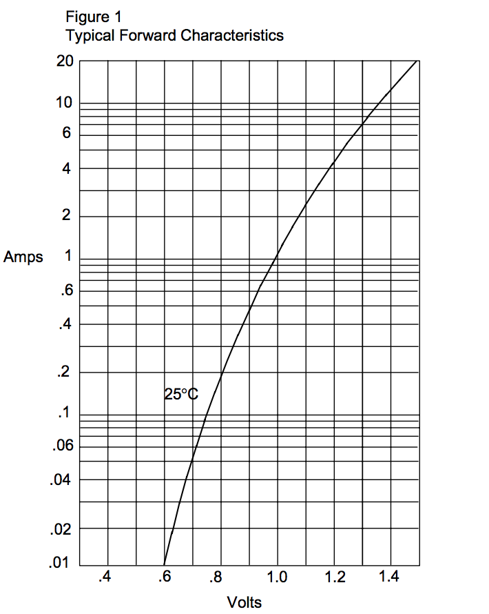
 (or close to) for a wide range of
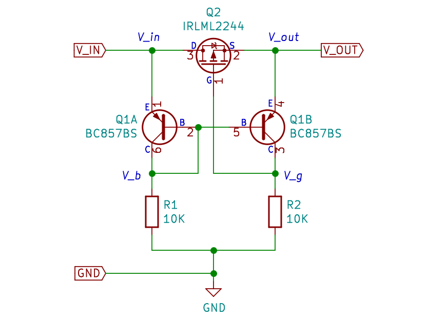
 and its source pin 2 provides the output voltage
  . This ensures that the MOSFET’s intrinsic diode is aligned in the direction of forward current flow and prevents any reverse current from flowing through it.
 at a gate-source voltage of
  and a drain current of
  (see
(see  at
at  .
. across the resistor R2.
 between the transistor’s base and the power supply ground:

 and
and  are the emitter-base voltages of transistors Q1A and Q1B. And:

 is the specified base-emitter voltage drop for BC857BS (see
  . A current can only flow through the emitter-base junction of Q1A or Q1B if the corresponding emitter-base voltage


 and cause the MOSFET Q1B to turn on.