Following is the tutorial of a DIY high accuracy Nixie Clock implemented on Arduino. It features a DCF77 receiver, alarm clock, timer, stopwatch, automatic brightness and more. The highlight feature being the ability of this clock to automatically calibrate its internal timer based on the received DCF77 signal, achieving an accuracy of less than 1 second a month at room temperature.
The purpose of this page is to help electronics enthusiasts around the world to build their own Nixie Clock by reusing the whole or part of the current design and software. I hope you find this material useful and would be happy to hear your feedback in the comment box at the bottom of this page.
Warning: Nixie tubes are powered by a dangerously high voltage of more than 170 Volts. The author of this page is not liable and takes no responsibility of any damage to living beings and things due to the implementation and usage of the Nixie clock. Please be aware that the current design has not been certified for safety, consequently it is not suitable for commercial applications and must be implemented at your own risk. Please do not attempt this project unless you are fully confident in what you are doing and do possess the required technical skills.
Table of Contents
About Nixie Tubes
A Nixie tube, or cold cathode display, is an electronic device for displaying numerals or other information using glow discharge. The glass tube contains a wire-mesh anode and multiple cathodes, shaped like numerals or other symbols. Applying power to one cathode surrounds it with an orange glow discharge. The tube is filled with a gas at low pressure, usually mostly neon and often a little mercury or argon.
The most common form of Nixie tube has ten cathodes in the shapes of the numerals 0 to 9 (and occasionally a decimal point or two), but there are also types that show various letters, signs and symbols. Because the numbers and other characters are arranged one behind another, each character appears at a different depth, giving Nixie based displays a distinct appearance. Some Russian Nixies, e.g. the ИH-14 (IN-14), used an upside-down digit 2 as the digit 5, presumably to save manufacturing costs as there is no obvious technical or aesthetic reason.
Each cathode can be made to glow in the characteristic neon red-orange color by applying about 170 volts DC at a few milliamperes between a cathode and the anode. The current limiting is normally implemented as an anode resistor of a few tens of thousands of ohms.
Nixie tubes suffer from an effect called “Cathode Poisoning”. Whereas the cathodes of the digits that are not being regularly lit get contaminated by deposits emerging from more frequently lit neighboring digits. These deposits eventually lead to the partial or total failure of the affected cathodes. In oder to acoid cathode poisonoing, all the Nixie tube’s cathodes must be powered-on at regular intervals.
Hundreds of variations of this design were manufactured by many firms, from the 1950s until the 1990s when they were displaced from the market by the LED and LCD displays.
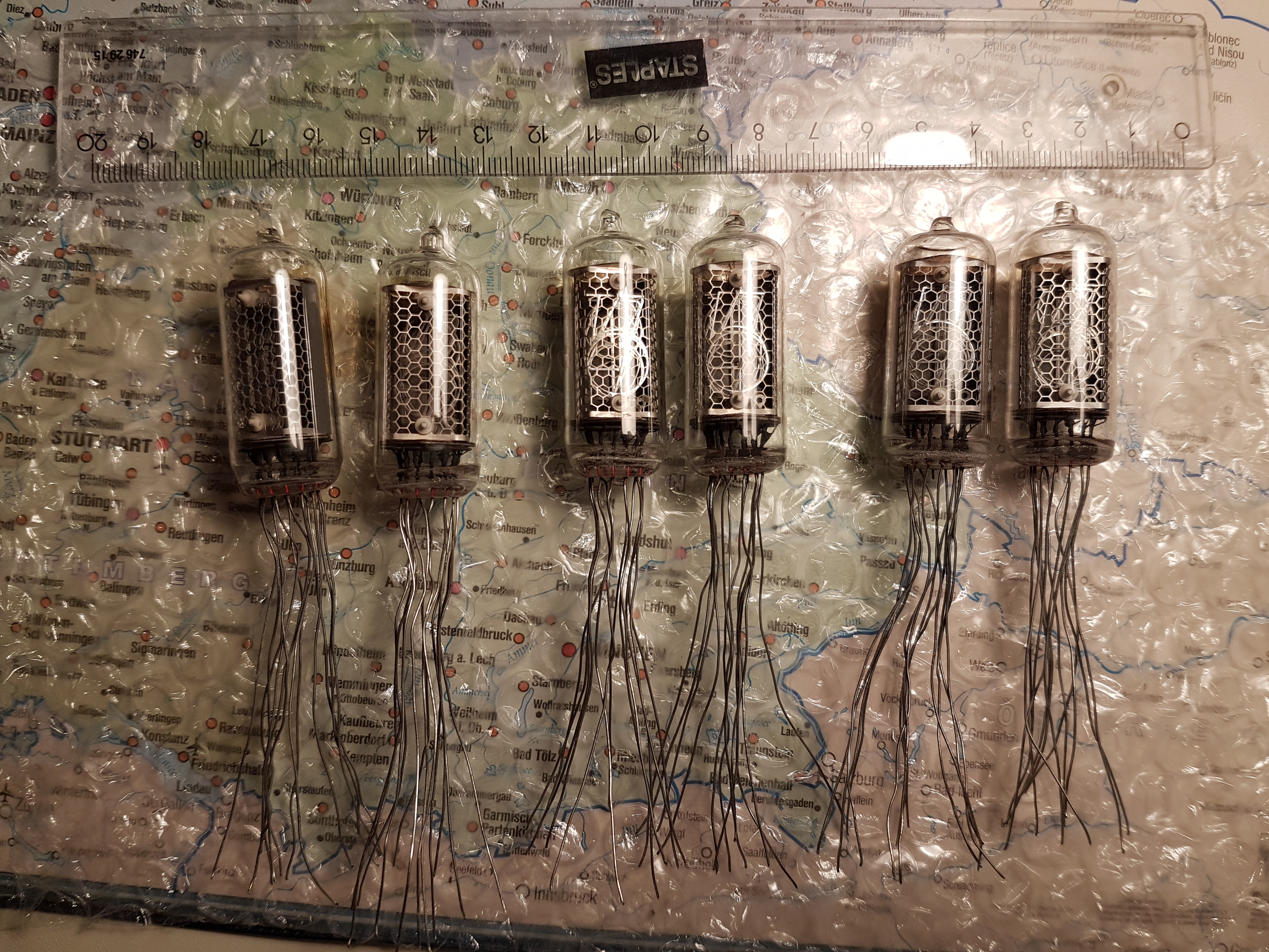
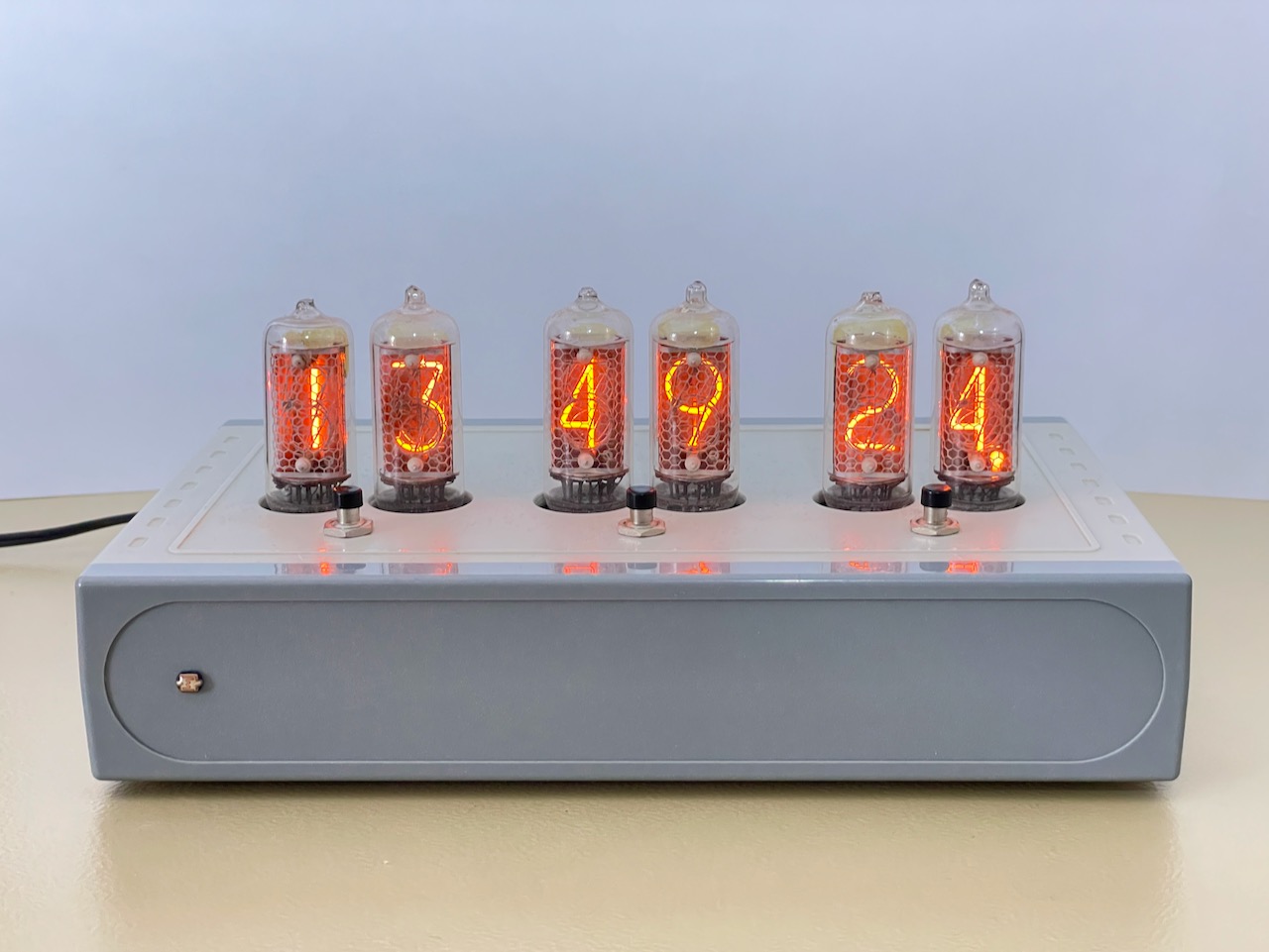
The Nixie Clock is built around six IN-8-2 Soviet-made Nixie tubes shown in the above picture. This kind of tubes can display digit values from 0 to 9, complemented by a decimal point at the bottom-right side of the digit. These were produced at the Melz Tube Factory in Moscow. In contrast to other Soviet tubes (like the IN-14), these tubes have slightly larger digits relative to the overall tube height and don not use an inverted “2” for the digit “5”. According to the imprint on their back, the particular samples used for this project are dated 1974 and are still running good.
Features
The Nixie Clock runs off a 12 Volt power supply, however the Nixie tubes require a high anode voltage of approximately 180 Volts DC. The 12 Volts are up-converted using an off-the-shelf DC-DC converter. This ensures an adequate galvanic separation from the mains power supply. The tubes cathodes are driven by a K155ID1 cathode driver IC, which is a BCD-to-decimal decoder especially designed for this purpose. Each of the anodes is driven via a dedicated optocoupler (TLP 127).
The clock’s CPU is an Atmel ATmega328P microcontroller which runs on an off-the-shelf Arduino Pro Mini compatible board. The CPU has a clock frequency is 16 MHz, 2 Kilobytes of RAM and 1 Kilobyte of EEPROM. It features two separate programmable timers. Timer 1 is used for the main timekeeping, while lower resolution Timer 2 supplies the clock signal for the Countdown Timer and Stopwatch features.
The microcontroller drives the Nixie tubes via multiplexing. Which means that only one Nixie tube can be lit at any single moment in time. One single K155ID1 cathode driver chip is used for driving the cathodes of the tubes in parallel. Each of the anodes is individually driven using its own optocoupler. The microcontroller quickly cycles through the individual digits, while the persistence of the human vision creates the illusion that all the digits are being simultaneously lit.
The brightness of the Nixie tubes is automatically adjusted to match the ambient lighting conditions. A photoresistor is used for measuring the ambient light intensity. Brightness is controlled by varying the power-on duty cycle of the Nixie tubes.
To avoid cathode poisoning, the Nixie Clock ensures that all the digits are being periodically lit by using one of the Cathode Poisoning Prevention routines.
This clock has a built-in receiver for the DCF77 time signal. DCF77 is a German longwave time signal and standard-frequency radio station. It started service as a standard-frequency station on 1 January 1959. In June 1973 date and time information was added. Its primary and backup transmitter are located at 50°0′56″N 9°00′39″E in Mainflingen, about 25 km south-east of Frankfurt am Main, Germany. The transmitter generates a nominal power of 50 kW, of which about 30 to 35 kW can be radiated via a T-antenna. The DCF77 signal can be received within a range of around 2000 km away from the transmitter.
The time keeping is based on the 16 MHz quartz oscillator of the Arduino Pro Mini. If used without any compensation measure, this oscillator is rather inaccurate would yield to a clock drift of the order of tens of seconds per day. The Nixie Clock features a calibration algorithm that actively compensates for this clock drift by periodically adjusting the Arduino’s Timer1 frequency against the received DCF77 time signal. When fully calibrated and at a relatively constant room temperature, this clock can achieve an impressive accuracy of lass than 1 second a month without the need to perform any further DCF77 receptions. This makes it comparable to some top of the range high accuracy quartz watches.
The Nixie Clock uses a supercapacitor to provide backup power for the event of a main power loss. Once main power is disconnected, the microcontroller backs-up all the settings to EEPROM and switches to a power-saving mode while continuing the timekeeping with the usual accuracy. Once the supercapacitor voltage drops below a certain threshold, the microcontroller switches into the next level of power saving by powering down most of the hardware peripherals, including Timer 1 which is used for the main timekeeping; timekeeping will continue with a reduced accuracy using the watchdog hardware.
Following is the full list of the Nixie Clock features:
- Arduino Pro Mini: Atmel ATmega328P, 16 MHz, 2 KB RAM , 1 KB EEPROM, 14 GPIO, 8 ADC inputs
- 6 IN-8-2 Nixie tubes featuring 0-9 digits and decimal points
- Multiplexed display, requires one single K155ID1 Nixie driver chip
- Synchronization with the DCF77 time signal
- Automatic oscillator calibration against the DCF77 time signal with 1/64 microsecond accuracy
- Multiple time zone support with manual or automatic daylight saving time
- Backup power from a built-in supercapacitor
- Dual timers: Timer1 used for timekeeping and Timer2 for countdown timer / stopwatch
- Automatic and manual display brightness adjustment
- Menu navigation using 3 push-buttons
- Alarm clock with the weekday and weekend options
- Countdown timer
- Stopwatch
- Service menu
- Cathode poisoning prevention and the “Slot Machine” effect
- Screen blanking with dual time intervals
- Settings are stored to EEPROM
Hardware
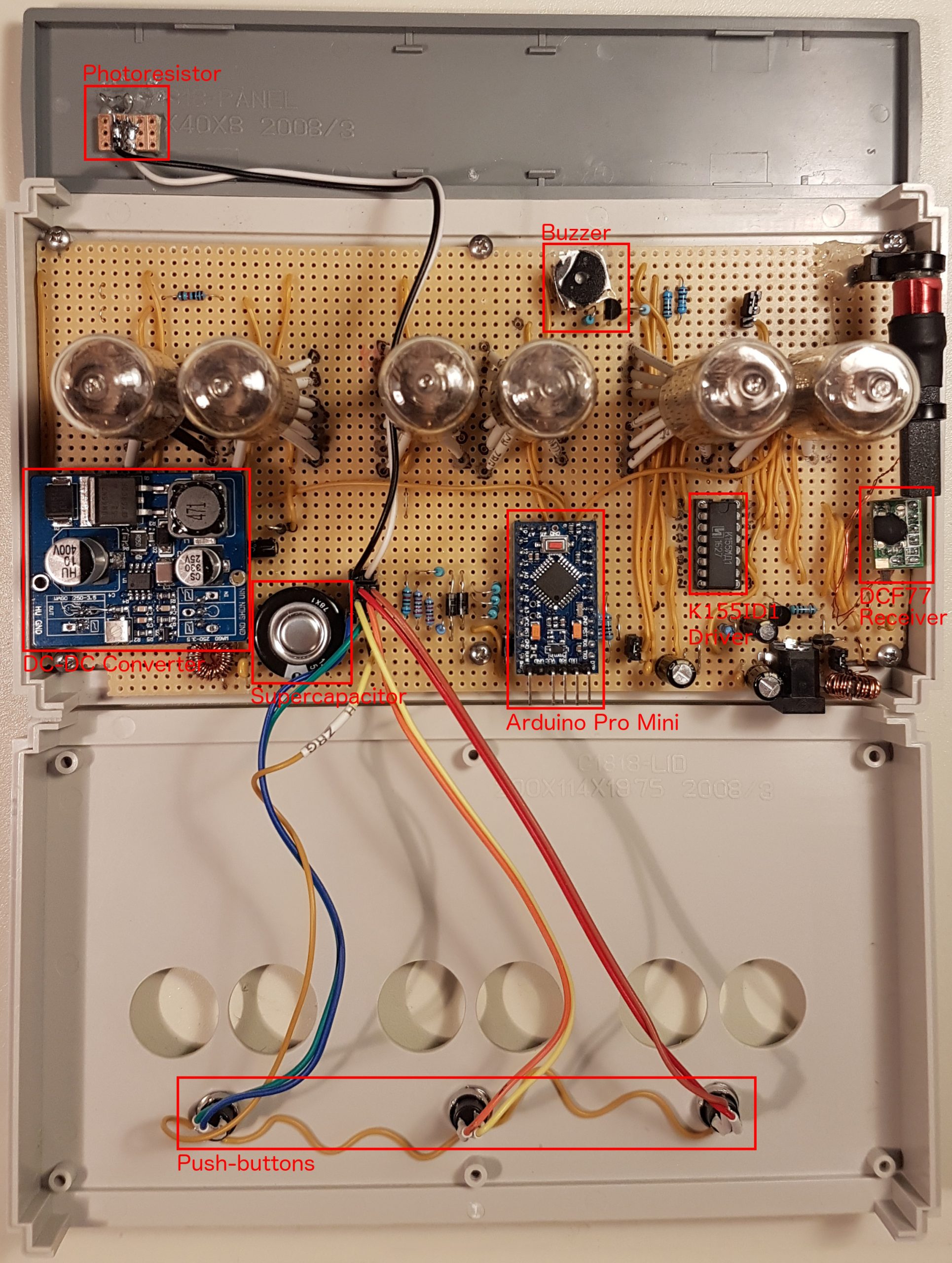
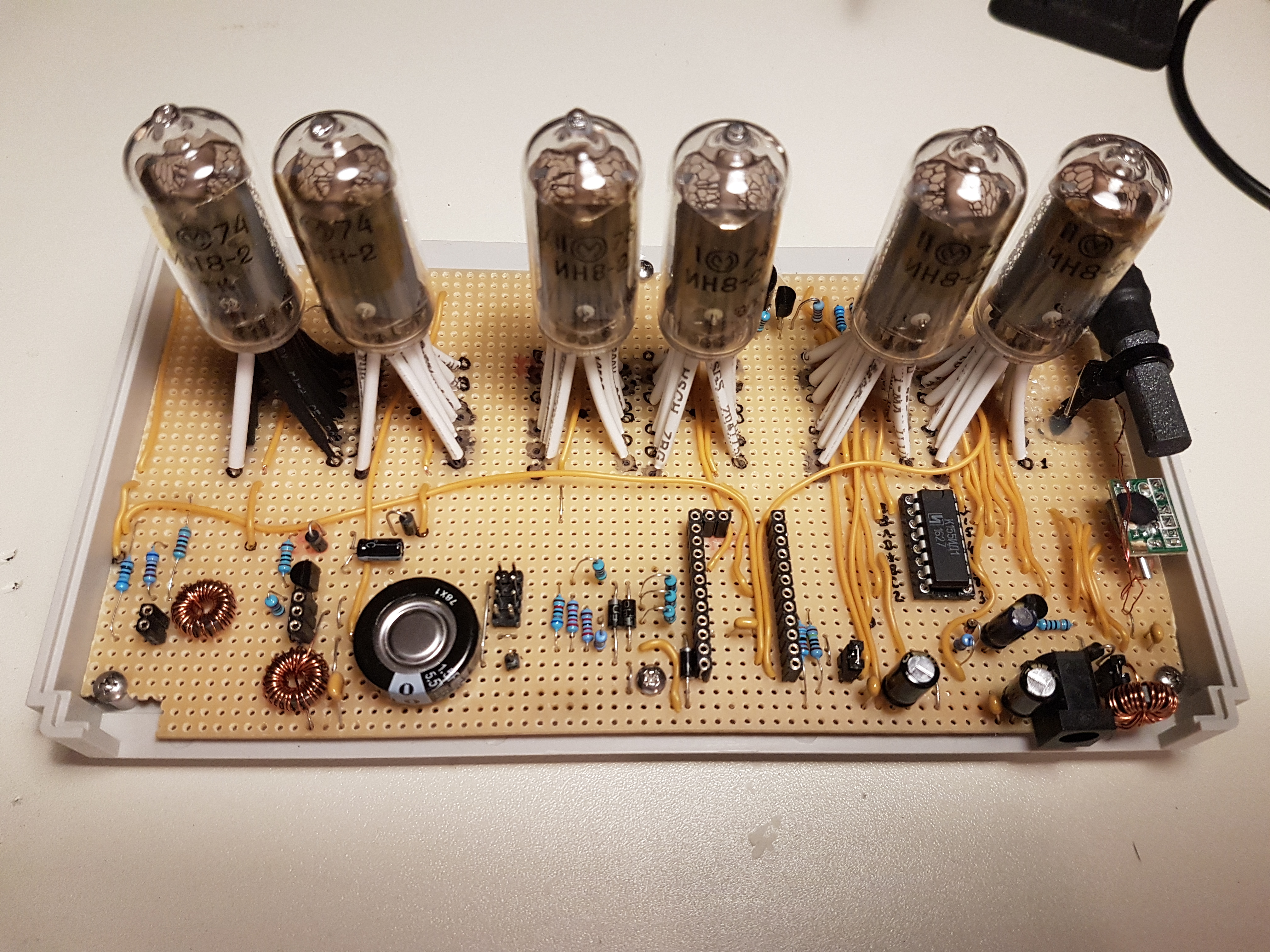
The Nixie Clock consists of the following hardware components as seen on the picture below:
- Nixie tubes
- Arduino Pro Mini board
- DC-DC converter board
- DCF77 reciever board with antenna
- K155ID1 Nixie tube driver IC
- Supercapacitor
- Photoresistor
- Buzzer
- Push-buttons
The clock has been designed around an off-the-shelf enclosure of type “RND 455-00121” with the dimensions of 200 x 121 x 40 mm.
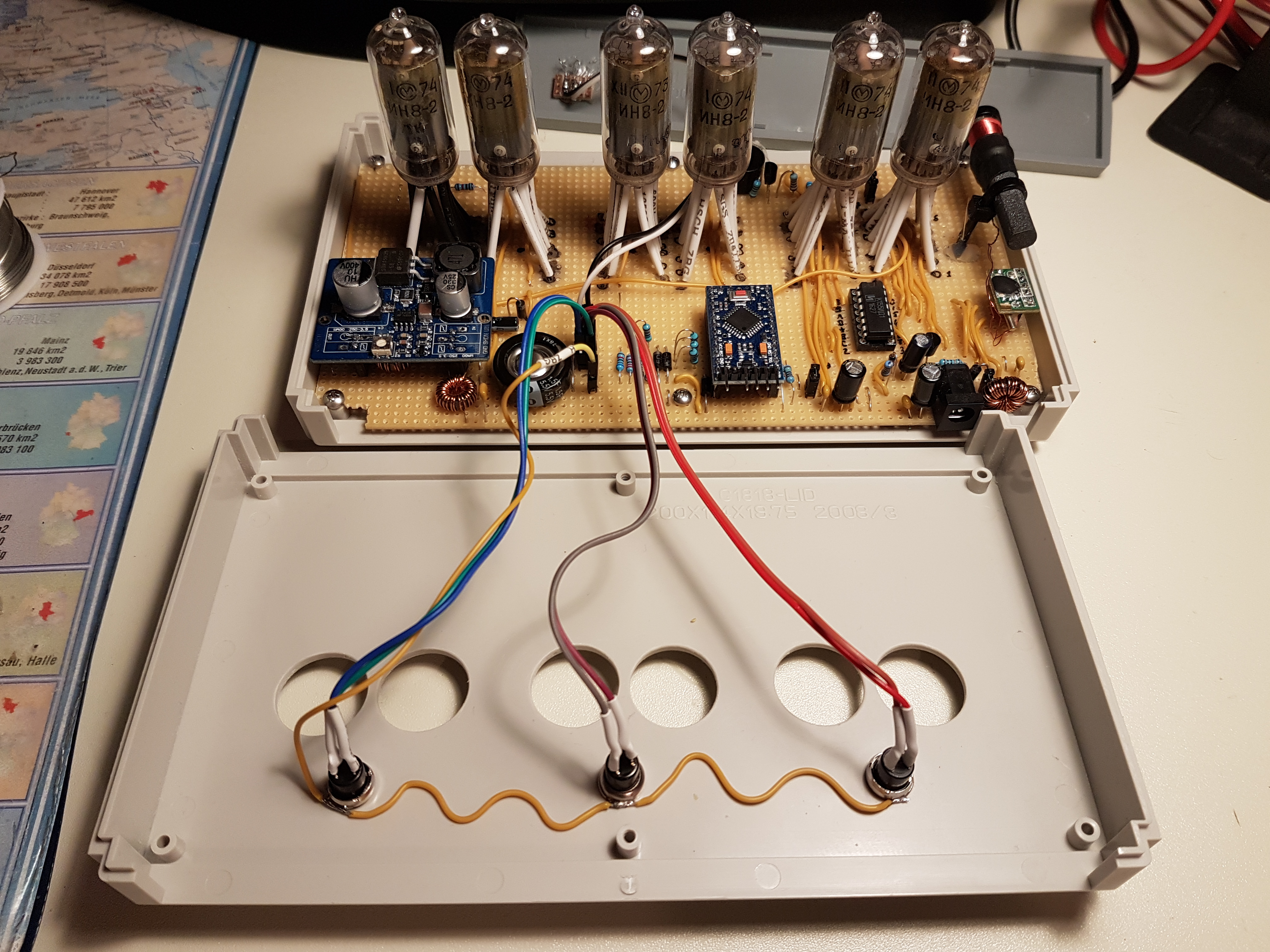
The following picture shows the open enclosure of the Nixie Clock with various components marked in red color.
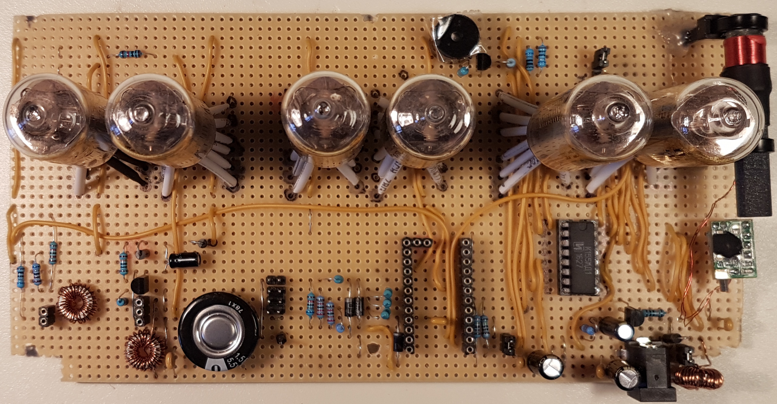
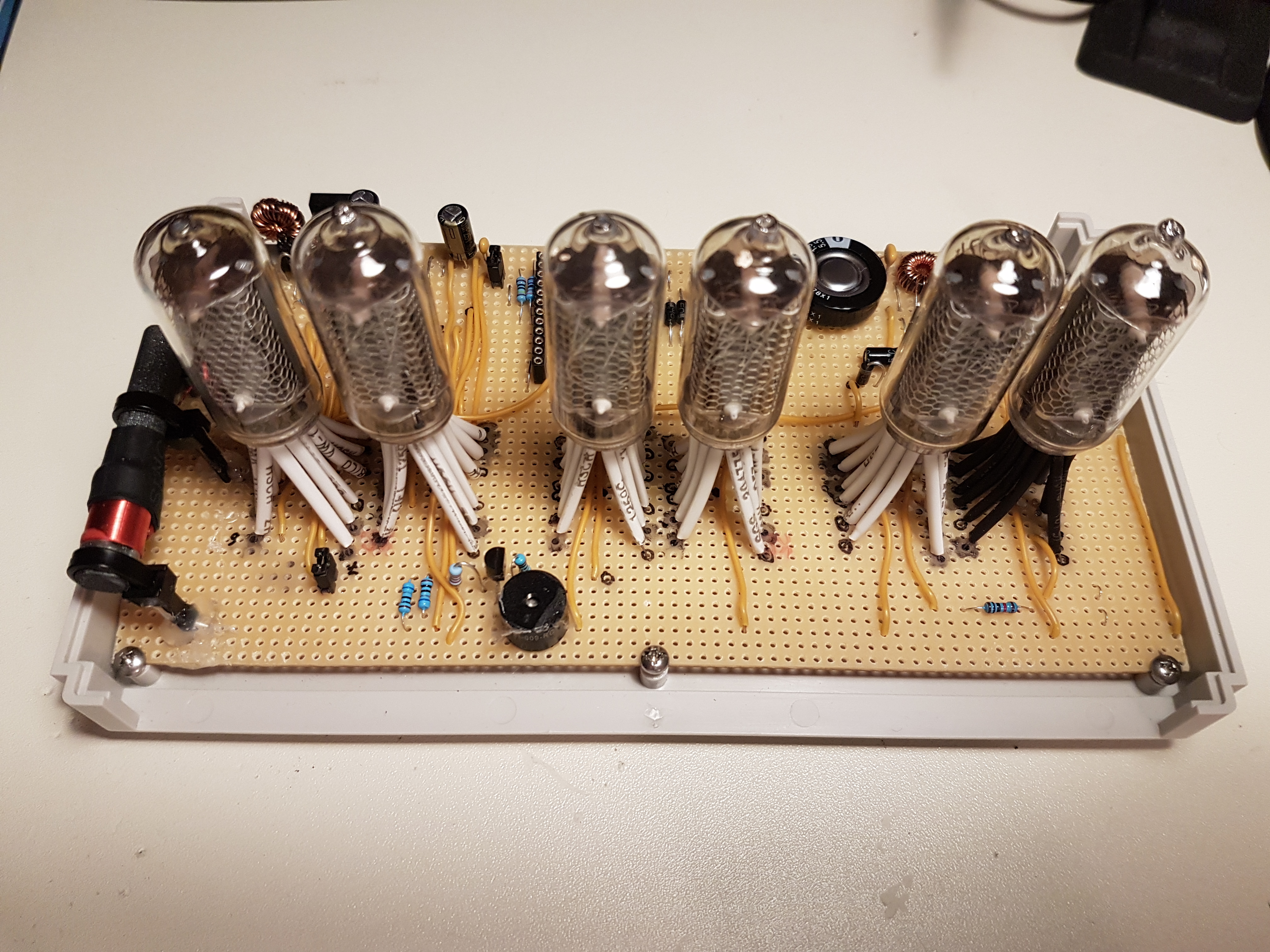
The circuit has been assembled on a stripboard PCB with most of the components mounted on the top side; except for the optocouplers, voltage regulator and a couple of resistors which are soldered to the bottom side of the PCB. The following picture show the top side of the PCB where the DC-DC converter and Arduino boards have been removed. Note that there is a 220 nF ceramic capacitor hidden under the socket of the K155ID1 IC.
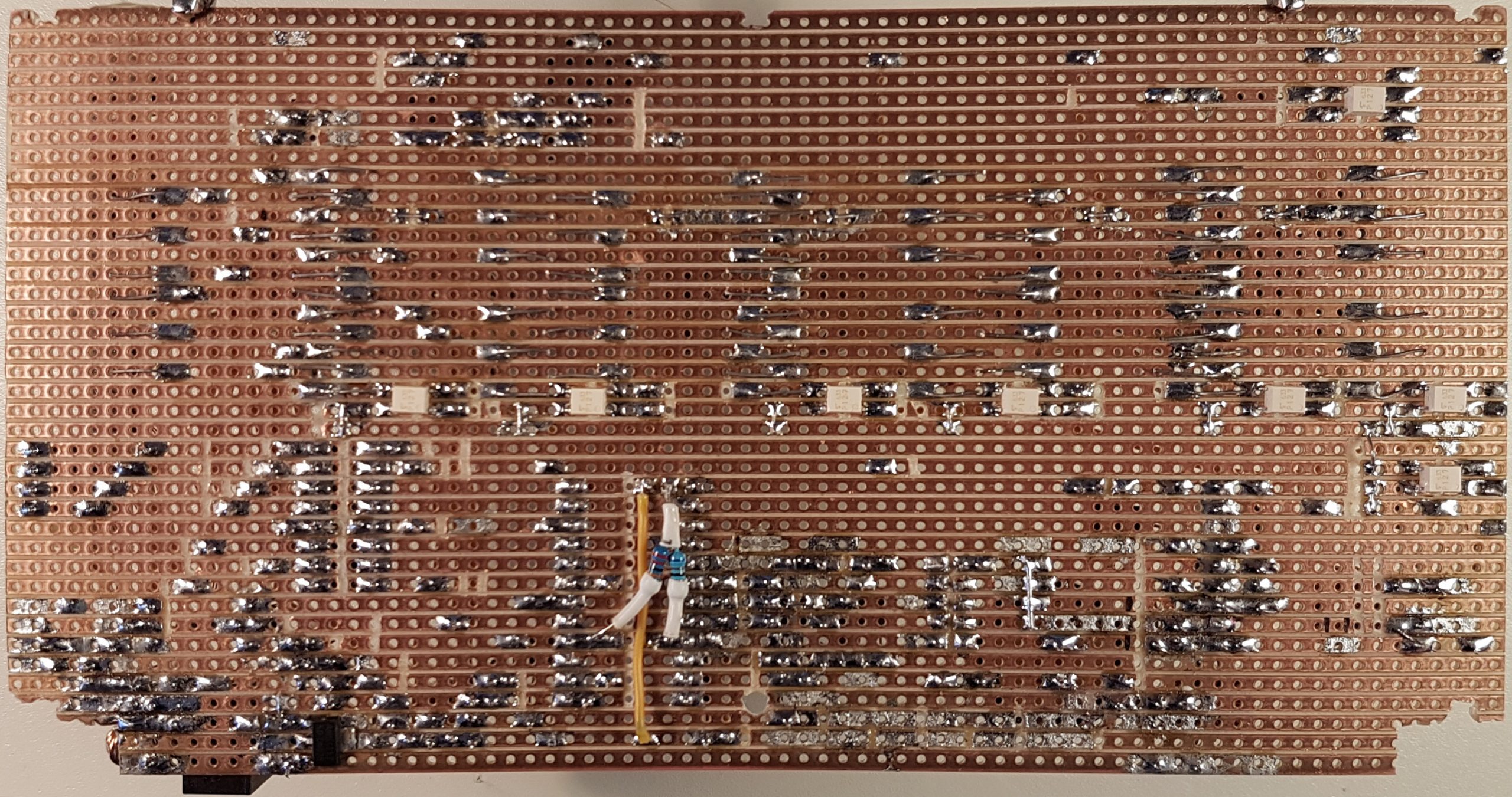
The following picture shows the bottom side of the PCB. Note the placement of the 8 optocouplers (in white) as well as the voltage regulator (bottom-left corner) and 2 resistors. Also note the locations where the copper lanes have been cut.
The following picture gallery shows the insides of the Nixie clock from different perspectives.
IN-8-2 Nixie Tube
The following figures show the outline and pinout of the IN-8-2 Nixie tube (source: www.tube-tester.com/sites/nixie/data/I/IN-8-2/in-8-2.htm).
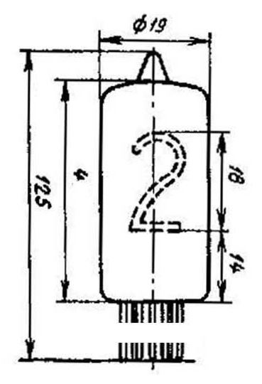
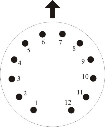
| Pin | Connection |
| 1 | Cathode digit 1 |
| 2 | Cathode digit 2 |
| 3 | Cathode digit 3 |
| 4 | Cathode digit 4 |
| 5 | Cathode digit 5 |
| 6 | Cathode digit 6 |
| 7 | Cathode digit 7 |
| 8 | Cathode decimal point |
| 9 | Cathode digit 8 |
| 10 | Cathode digit 9 |
| 11 | Cathode digit 0 |
| 12 | Anode |
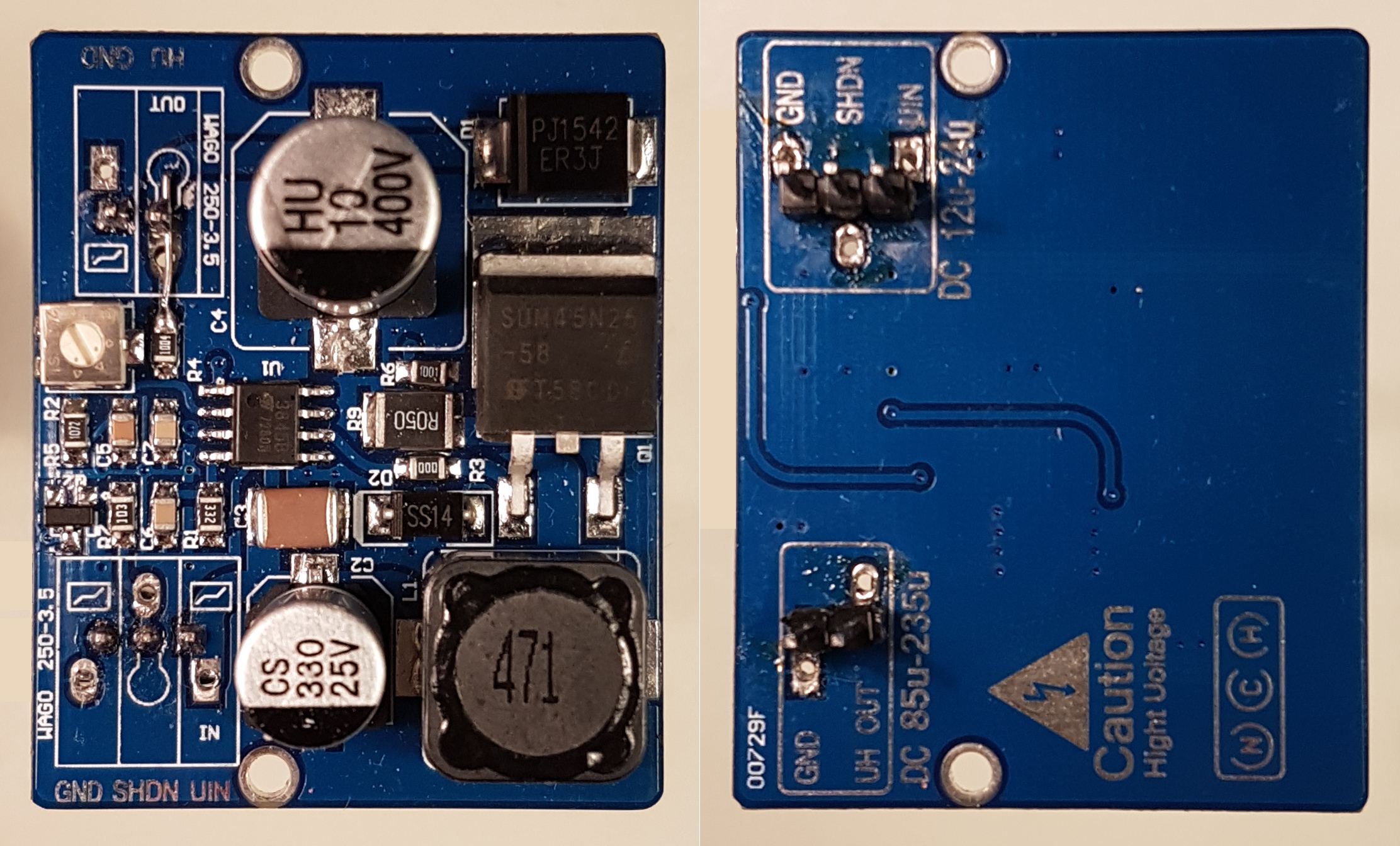
DC-DC Converter
The figure below shows a close-up image of the high-voltage DC-DC converter.
The current device has been running for 5000+ hours and has proven to be very reliable and silent.
Arduino
An Arduino Pro Mini clone with the following modifications has been used in this project:
- in order to reduce power consumption and increase backup power runtime, the onboard power LED and voltage regulator have been desoldered as shown in the following link: https://andreasrohner.at/posts/Electronics/How-to-modify-an-Arduino-Pro-Mini-clone-for-low-power-consumption/
- A custom bootloader with watchdog timer support has been flashed as shown in the following link: https://github.com/microfarad-de/bootloader
Note that there are Arduino Pro Mini boards using a quartz oscillator as well as those using a cheaper a resonator as a CPU clock source. For best clock accuracy over a wider range of ambient temperatures, It recommend to use a quartz oscillator driven Arduino board. (The above pictures show a resonator driven Arduino board, whereas the quartz oscillator has two pins and is much larger in size, as opposed to the barely visible three pin resonator.)
Furthermore, the use of an Arduino Nano (essentially an Arduino Pro Mini with an onboard USB to Serial converter chip) is not recommended as its onboard USB to serial converter would significantly increase the power consumption, thus reduce the runtime on backup power from the super capacitor. It may also interfere withe the buzzer and brightness boost features connected to the RXI and TXO pins that are also being used for serial communication.
Circuit Diagram
The figure below shows the schematic of the Nixie Clock.
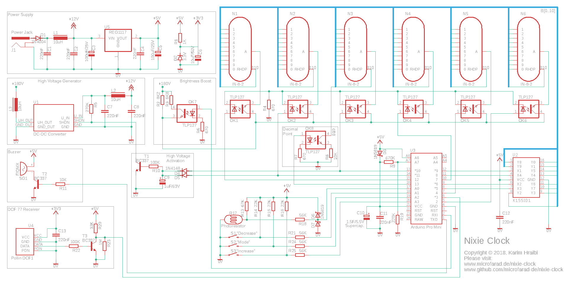
It consists of the following blocks:
- Power supply: generates the voltages required for powering-up the various sub-systems. It uses the AMS1117 (U5) linear regulator for the 5 Volts output and a Zener diode (D2) for the 3.3 Volts.
- High voltage generator (U1): generates the Nixie tube anode voltage of approximately 180 Volts. It uses an off-the-shelf DC-DC converter which was purchased from China on Ebay.
- High voltage activation circuit (T1, D4, D5, C9, R10): as soon as the ATmega microcontroller begins driving the Nixie tube anodes, this circuit detects the periodic pulses on the anodes of tubes N2 and N3 and subsequently enables the high voltage output on the DC-DC converter (U1).
- Brightness boost circuit (R2, R3, R6, OK7): increases the Nixie tube brightness by reducing the value of the anode resistor. This is an exceptional measure for very bright daylight conditions as the brightness is normally controlled via Pulse Width Modulation (PWM).
- DCF77 receiver (U4): contains the “Pollin DCF1” receiver which runs at 3.3 Volts, has a very low power consumption (as it is designed for battery-powered clocks) and has very high output impedence. An NPN transistor (T3) is used for boosting the output signal and making it suitable for the ATmega microcontroller’s input pin.
- Buzzer (SG1): includes an NPN transistor (T2) buffer stage for the buzzer
Further, the schematic contains the following items:
- 6 Nixie tubes (N1 to N6), the optocouplers (OK1 to OK6) for driving the anodes and the decimal point cathode (OK8); and the K155ID1 (U2) cathode driver chip for driving the digit cathodes
- Backup power circuit with a Schottky diode (D3) and a supercapacitor (C10)
- Photoresistor (R17), push-buttons (S1, S2, S3) with their pull-up resistors (R13 to R16) and related input protection circuitry. Notice that due to the shortage of digital pins, the three push-buttons are actually connected to the left-over analog pins. Also note the lack of any debouncing circuitry as button debouncing is being performed in software.
- Three 10 µH (L1, L2, L3) inductors have been placed around the circuit, one standalone and two as part of low-pass networks. These are required for suppressing the high-frequency noise of the DC-DC converter and the 12 Volt switching power supply. Failing to do so would significantly reduce the performance of the DCF77 receiver which is overly sensitive to electrical noise.
Some Electrostatic Discharge (ESD) protection measures have been taken in order to protect the Arduino’s ATmega microcontroller. The push-buttons and the photoresistor are especially prone to for taking ESD due to their location on the outside of the enclosure, the frequent user interaction and their direct connection to with the Arduino’s ADC pins.
In order to prevent ESD damage, the metal bodies of the push-buttons (S1, S2, S3) have been connected to the negative power supply (not shown on the schematic) and current-limiting resistors (R21, R24, R25) have been connected in series with the ADC inputs. This will ensure that any ESD discharge would be diverted to the negative power supply through the bodies of the switches and any residual current is limited by the resistors.
ESD protection of the photoresistor (R17) has been achieved via a current-limiting resistor (R18) in conjunction with a pair of clamping diodes (D6, D7). The clamping diodes deflect the excess voltage due to an ESD event towards the positive and negative power rails, ensuring that the voltage at the analog input pin stays within the range from -VD to VCC + VD. Whereas VD is the junction voltage of the diode (0.3 V for the used Schottky diode) and VCC is the +5 V power supply voltage. The current-limiting resistor protects the clamping diodes from being destroyed by the ESD current pulse.
Notice some minor discrepancies between the below schematic and the pictures shown in the previous section. The schematic shows a couple of additional filtering capacitors (C1, C8) and better-suitable diode types (D4, D5). The schematic does not show any of the jumpers and pin headers present on the PCB.
The above schematic has been implemented using Autodesk Eagle, the related source files can be found under the downloads section below. Please note that the PCB layout has not been yet finalised, however i would be very happy if someone would find the time to contribute.
Downloads
Among others, below you can find GitHub download links for the Arduino firmware source code, user manual and the Eagle schematic source files. All the source code is distributed under the GNU General Public License v3.0.
Please note that the current implementation uses the watchdog timer functionality which requires the customized Arduino bootloader found under the link below. Additionally, ensure that you use Arduino IDE version 1.8.19 to compile the firmware. For more details, please follow the installation instructions found within the README file on GitHub.
Hey Karim, thanks so much for your reply. I tried commenting lines 1142 to 1154 but I get the same effect after a power disconnection: Arduino doesn’t wake up.
Yes, I flashed the custom bootloader using Atmel studio and a mkII adapter.
Other strange behaviors I can report:
– decimal point 5 is always ON, even if I set parameters 2.1 and 2.2 to 0 (DCF OFF and live signal indicator ->> OFF)
– DCF77 doesn’t seem to work but maybe it’s because a lack of radio signal
– when I reconnect the power (and currently press reset to wake up Arduino) it always starts counting from 01:00:00, (UTC setting is currently +1). Is this normal or should it remember the previous shutdown time?
In general the parameters are correctly saved in the eeprom and are kept even after power disconnections.
Finally, I would like to show you my creation, can you tell me an email address to send you some photos? I mastered two PCBs for this project, one as a backplane for the tubes, another for the controller, plus I built a wooden enclosure.
Marco
Hi Marco,
having read your comment, I suspect that you have some issue with the DCF77 receiver circuit. Could you please measure the voltage at Arduino PIN 3 to ensure that it corresponds to 5 V when 9 V power is connected?
The DCF signal indicator (second decimal point from the right) is handled at nixie-clock.ino line 553. It should be completely disabled if dcfSyncActive = false.
The Nixie clock relies on the supercap for saving the time during power outage, so the current time is never saved to EEPROM. For UTC+1, you are expected to see 01:00:00 upon startup.
Of course, I would be happy to see some pictures of your implementation, please send them to microfarad.de (at) gmail.com.
Thanks, Karim
Hi Karim,
I’ve finished building the clock, it works but not completely, I have a strange problem: when I disconnect the power (9V in my case), Arduino is kept on by the super cap while the tubes and the other circuits turn off: it’s normal. When I reconnect the power supply Arduino remains in a sort of idle state and the tubes does not switch on. The only way to get everything working is to press the reset button on arduino… why? any idea? I’m using arduino nano.
Thanks in advance
Marco
Hi Marco,
good to hear that you have finished the project. When 9V power gets disconnected, the Arduino goes through two levels of power saving sleep modes which are implemented in the powerSave() function within nixie-clock.ino line 1101. The first sleep stage “light sleep” occurs when DCF_PIN (pin 3) goes low due to the lack of 9 V (or 12 V) supply. The second sleep stage “deep sleep” occurs as soon as the measured super capacitor voltage at VOLTAGE_APIN (pin A7) becomes lower than voltageThreshold = 800, which corresponds to approximately 3.5 V in my case.
As a first step, I would try to completely disable the deep sleep mode by commenting out nixie-clock.ino lines 1142 thru 1154. Thus, by removing the conditional statement that check the supercap voltage. Could you please try this and let me know if the Arduino wakes up?
Best regards
Karim
By the way, did you flash your Arduino with the customized bootloader for watchdog timer support as described in https://github.com/microfarad-de/bootloader? If not, this could be one reason why the Arduino hangs since the deep sleep mode configures a watchdog timer as the source for the seconds tick.
Hi Karim,
Giacomo again. I have a question about the schematic diagram, about the “high voltage activation circuit”. Is C9 intended to work in inverted polarization? There’s a “-” marking near C9, but in the opposite side than GND… it’s a graphical error?
How does your DC DC enable input works? (SHDN pin)
mine is working in this way: HIGH=ON / LOW=OFF
Because it’s not very clear to me how does your circuit works… when you activate the anode of N2 and/or N3 you consequently put the SHDN pin at GND by activating T1.
So in my specific case you shut down the HV when the anode is supposed to be ON..
Maybe your DC DC works opposite than mine? HIGH=OFF / LOW=ON?
Thanks a lot
Hi Giacomo,
I have fixed the mistake in the schematic, the negative side of C9 must be connected to ground.
The enable (SHDN) pin on my DC-DC converter is active low. So whenever the anodes are being activated, a voltage will appear across C9 which will connect the SHDN pin to ground via T1 and consequently enable the DC-DC. If the Nixie display is turned off, the anode activation pulses will stop and SHDN will be pulled up via R5 and DC-DC gets disabled. This circuit spares us the use of a dedicated Arduino output pin for controlling the DC-DC. You could as well skip this circuit by keeping DC-DC enabled at all times.
Best regards,
Karim
Hi, I started building this awesome clock, thanks for sharing.
Two questions:
1) it’s not clear to me how you calculated the anode resistor. Since the datasheets of the IN-8-2 reports a max cathode current of 2,5mA, I suppose R2 should be around 70K… how did you calculate the value of 8,2K? With this value you get an anode current of 180/8200= 22mA. When OK7 switches ON the series resistor drops down to (8K2 // 6K8) = 3K7 and the current goes up to 48mA… aren’t these currents too high? Sorry if I wrote something stupid but I’m not confident with nixie tubes driving or maybe I don’t understand how do you drive the current.
2) I’m going to use IN-14 tubes instead of IN-8-2, because they are a little larger. The recommended anode voltage is 170V (I will use a proper DC DC) and the cathode current is the same as your tubes: 2,5mA. I will change the schematic accordingly to the pinout of the IN-14 that is slightly different from the IN-8-2. The IN-14 has two decimal points and I thought to use both by short circuit the pins and drive them togheter. In this case I suppose I have to double the current that flows through R8, is that right?
Thank you very much!
Hi Giacomo,
glad to hear from you and you are welcome. Answering your questions:
1) The Nixie tubes are driven by PWM and are multiplexed, so the average cathode current is significantly less than what you have calculated. At maximum intensity, the average cathode current is actually less than 22 / 6 = 3.67 mA. There are discussions whether PWM pulses exceeding the nominal current are good for the life of the Nixie tubes. My experience tells that the Nixie clock has been running for more than 5 years and 30K hours and the Tubes are still good as new. However I have to tell you that I don’t use the boost function very often, so the instantaneous current is about 22 mA as you have calculated.
2) Driving two cathodes in parallel through the same resistor would not lead to good results. Since the voltage drops across the anode and each of the cathodes are not exactly the same, one of them will glow brighter than the other. In this case I would recommend implementing a second circuit consisting of OK7, R7 and R8 and drive both decimal points independently.
Best regards, Karim