Following is the tutorial of a DIY high accuracy Nixie Clock implemented on Arduino. It features a DCF77 receiver, alarm clock, timer, stopwatch, automatic brightness and more. The highlight feature being the ability of this clock to automatically calibrate its internal timer based on the received DCF77 signal, achieving an accuracy of less than 1 second a month at room temperature.
The purpose of this page is to help electronics enthusiasts around the world to build their own Nixie Clock by reusing the whole or part of the current design and software. I hope you find this material useful and would be happy to hear your feedback in the comment box at the bottom of this page.
Warning: Nixie tubes are powered by a dangerously high voltage of more than 170 Volts. The author of this page is not liable and takes no responsibility of any damage to living beings and things due to the implementation and usage of the Nixie clock. Please be aware that the current design has not been certified for safety, consequently it is not suitable for commercial applications and must be implemented at your own risk. Please do not attempt this project unless you are fully confident in what you are doing and do possess the required technical skills.
Table of Contents
About Nixie Tubes
A Nixie tube, or cold cathode display, is an electronic device for displaying numerals or other information using glow discharge. The glass tube contains a wire-mesh anode and multiple cathodes, shaped like numerals or other symbols. Applying power to one cathode surrounds it with an orange glow discharge. The tube is filled with a gas at low pressure, usually mostly neon and often a little mercury or argon.
The most common form of Nixie tube has ten cathodes in the shapes of the numerals 0 to 9 (and occasionally a decimal point or two), but there are also types that show various letters, signs and symbols. Because the numbers and other characters are arranged one behind another, each character appears at a different depth, giving Nixie based displays a distinct appearance. Some Russian Nixies, e.g. the ИH-14 (IN-14), used an upside-down digit 2 as the digit 5, presumably to save manufacturing costs as there is no obvious technical or aesthetic reason.
Each cathode can be made to glow in the characteristic neon red-orange color by applying about 170 volts DC at a few milliamperes between a cathode and the anode. The current limiting is normally implemented as an anode resistor of a few tens of thousands of ohms.
Nixie tubes suffer from an effect called “Cathode Poisoning”. Whereas the cathodes of the digits that are not being regularly lit get contaminated by deposits emerging from more frequently lit neighboring digits. These deposits eventually lead to the partial or total failure of the affected cathodes. In oder to acoid cathode poisonoing, all the Nixie tube’s cathodes must be powered-on at regular intervals.
Hundreds of variations of this design were manufactured by many firms, from the 1950s until the 1990s when they were displaced from the market by the LED and LCD displays.
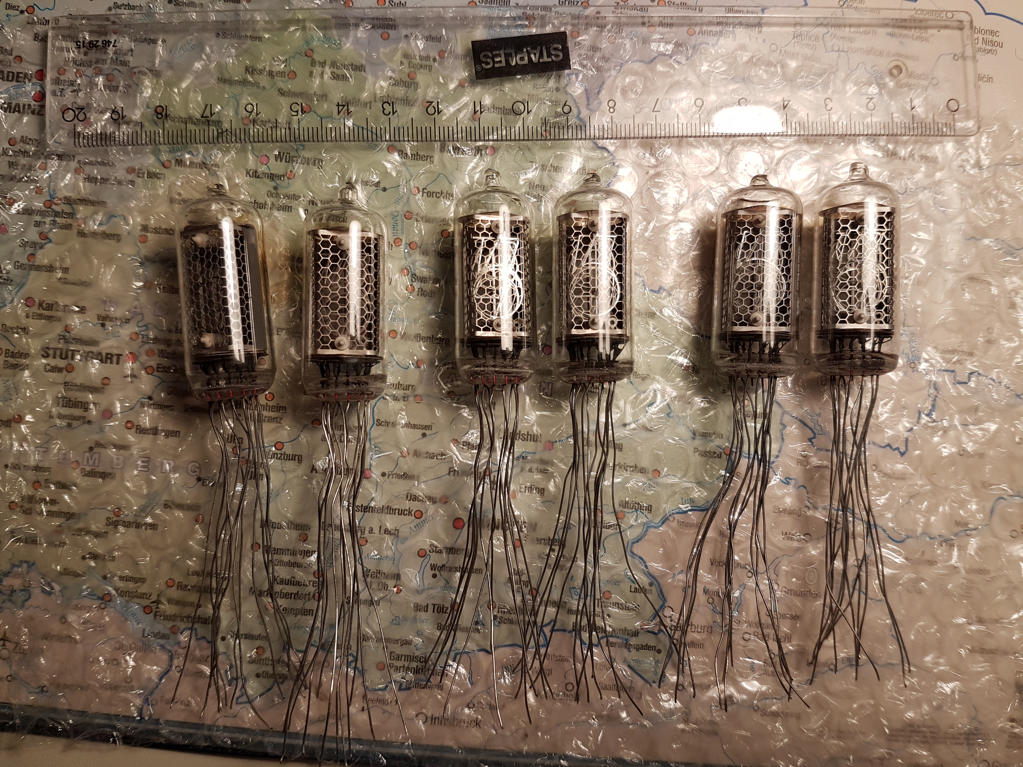
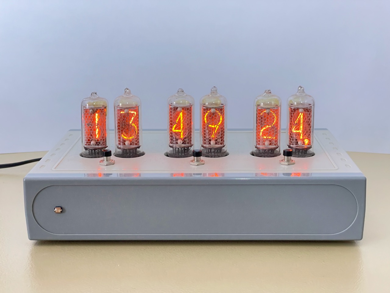
The Nixie Clock is built around six IN-8-2 Soviet-made Nixie tubes shown in the above picture. This kind of tubes can display digit values from 0 to 9, complemented by a decimal point at the bottom-right side of the digit. These were produced at the Melz Tube Factory in Moscow. In contrast to other Soviet tubes (like the IN-14), these tubes have slightly larger digits relative to the overall tube height and don not use an inverted “2” for the digit “5”. According to the imprint on their back, the particular samples used for this project are dated 1974 and are still running good.
Features
The Nixie Clock runs off a 12 Volt power supply, however the Nixie tubes require a high anode voltage of approximately 180 Volts DC. The 12 Volts are up-converted using an off-the-shelf DC-DC converter. This ensures an adequate galvanic separation from the mains power supply. The tubes cathodes are driven by a K155ID1 cathode driver IC, which is a BCD-to-decimal decoder especially designed for this purpose. Each of the anodes is driven via a dedicated optocoupler (TLP 127).
The clock’s CPU is an Atmel ATmega328P microcontroller which runs on an off-the-shelf Arduino Pro Mini compatible board. The CPU has a clock frequency is 16 MHz, 2 Kilobytes of RAM and 1 Kilobyte of EEPROM. It features two separate programmable timers. Timer 1 is used for the main timekeeping, while lower resolution Timer 2 supplies the clock signal for the Countdown Timer and Stopwatch features.
The microcontroller drives the Nixie tubes via multiplexing. Which means that only one Nixie tube can be lit at any single moment in time. One single K155ID1 cathode driver chip is used for driving the cathodes of the tubes in parallel. Each of the anodes is individually driven using its own optocoupler. The microcontroller quickly cycles through the individual digits, while the persistence of the human vision creates the illusion that all the digits are being simultaneously lit.
The brightness of the Nixie tubes is automatically adjusted to match the ambient lighting conditions. A photoresistor is used for measuring the ambient light intensity. Brightness is controlled by varying the power-on duty cycle of the Nixie tubes.
To avoid cathode poisoning, the Nixie Clock ensures that all the digits are being periodically lit by using one of the Cathode Poisoning Prevention routines.
This clock has a built-in receiver for the DCF77 time signal. DCF77 is a German longwave time signal and standard-frequency radio station. It started service as a standard-frequency station on 1 January 1959. In June 1973 date and time information was added. Its primary and backup transmitter are located at 50°0′56″N 9°00′39″E in Mainflingen, about 25 km south-east of Frankfurt am Main, Germany. The transmitter generates a nominal power of 50 kW, of which about 30 to 35 kW can be radiated via a T-antenna. The DCF77 signal can be received within a range of around 2000 km away from the transmitter.
The time keeping is based on the 16 MHz quartz oscillator of the Arduino Pro Mini. If used without any compensation measure, this oscillator is rather inaccurate would yield to a clock drift of the order of tens of seconds per day. The Nixie Clock features a calibration algorithm that actively compensates for this clock drift by periodically adjusting the Arduino’s Timer1 frequency against the received DCF77 time signal. When fully calibrated and at a relatively constant room temperature, this clock can achieve an impressive accuracy of lass than 1 second a month without the need to perform any further DCF77 receptions. This makes it comparable to some top of the range high accuracy quartz watches.
The Nixie Clock uses a supercapacitor to provide backup power for the event of a main power loss. Once main power is disconnected, the microcontroller backs-up all the settings to EEPROM and switches to a power-saving mode while continuing the timekeeping with the usual accuracy. Once the supercapacitor voltage drops below a certain threshold, the microcontroller switches into the next level of power saving by powering down most of the hardware peripherals, including Timer 1 which is used for the main timekeeping; timekeeping will continue with a reduced accuracy using the watchdog hardware.
Following is the full list of the Nixie Clock features:
- Arduino Pro Mini: Atmel ATmega328P, 16 MHz, 2 KB RAM , 1 KB EEPROM, 14 GPIO, 8 ADC inputs
- 6 IN-8-2 Nixie tubes featuring 0-9 digits and decimal points
- Multiplexed display, requires one single K155ID1 Nixie driver chip
- Synchronization with the DCF77 time signal
- Automatic oscillator calibration against the DCF77 time signal with 1/64 microsecond accuracy
- Multiple time zone support with manual or automatic daylight saving time
- Backup power from a built-in supercapacitor
- Dual timers: Timer1 used for timekeeping and Timer2 for countdown timer / stopwatch
- Automatic and manual display brightness adjustment
- Menu navigation using 3 push-buttons
- Alarm clock with the weekday and weekend options
- Countdown timer
- Stopwatch
- Service menu
- Cathode poisoning prevention and the “Slot Machine” effect
- Screen blanking with dual time intervals
- Settings are stored to EEPROM
Hardware
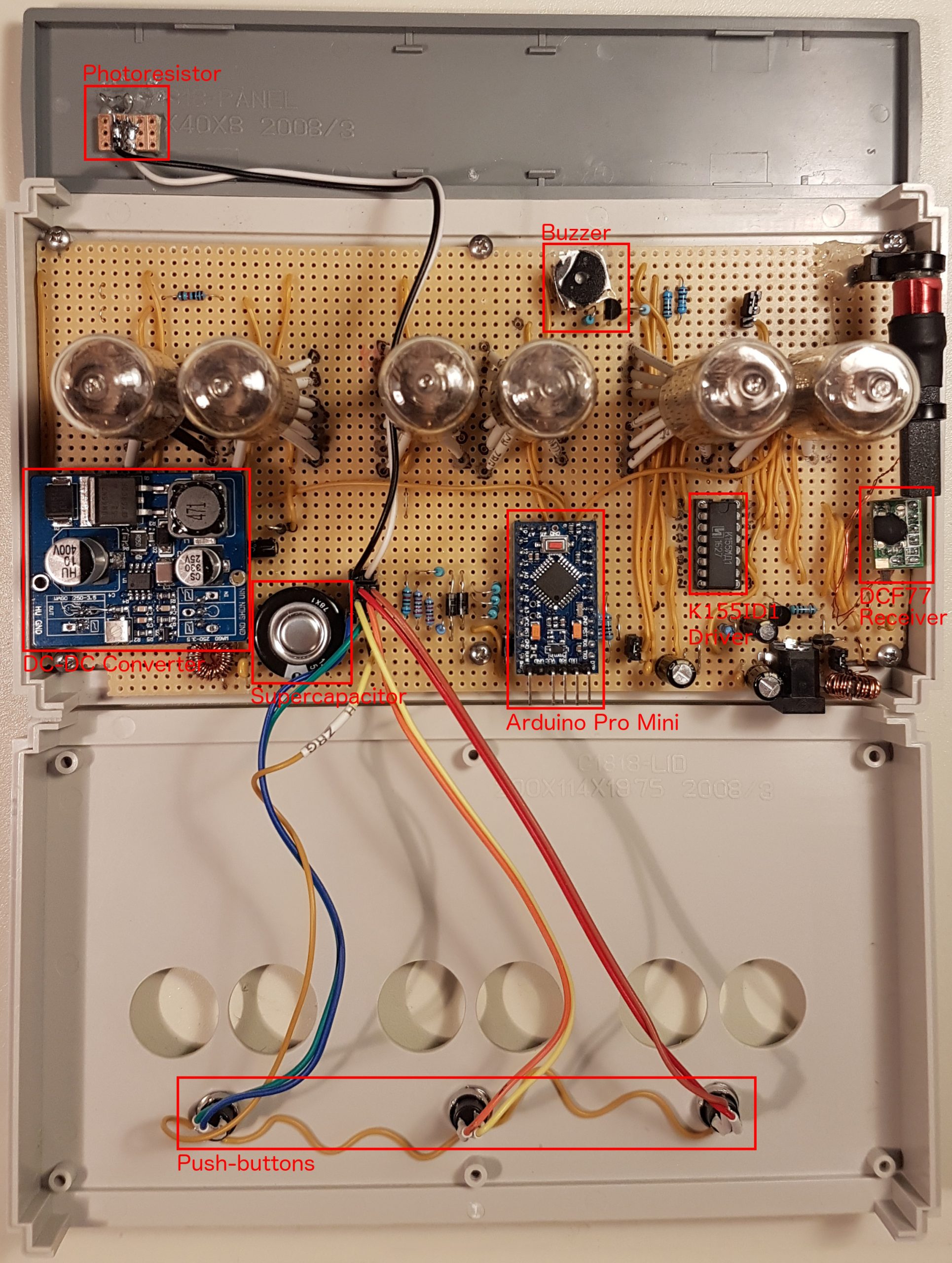
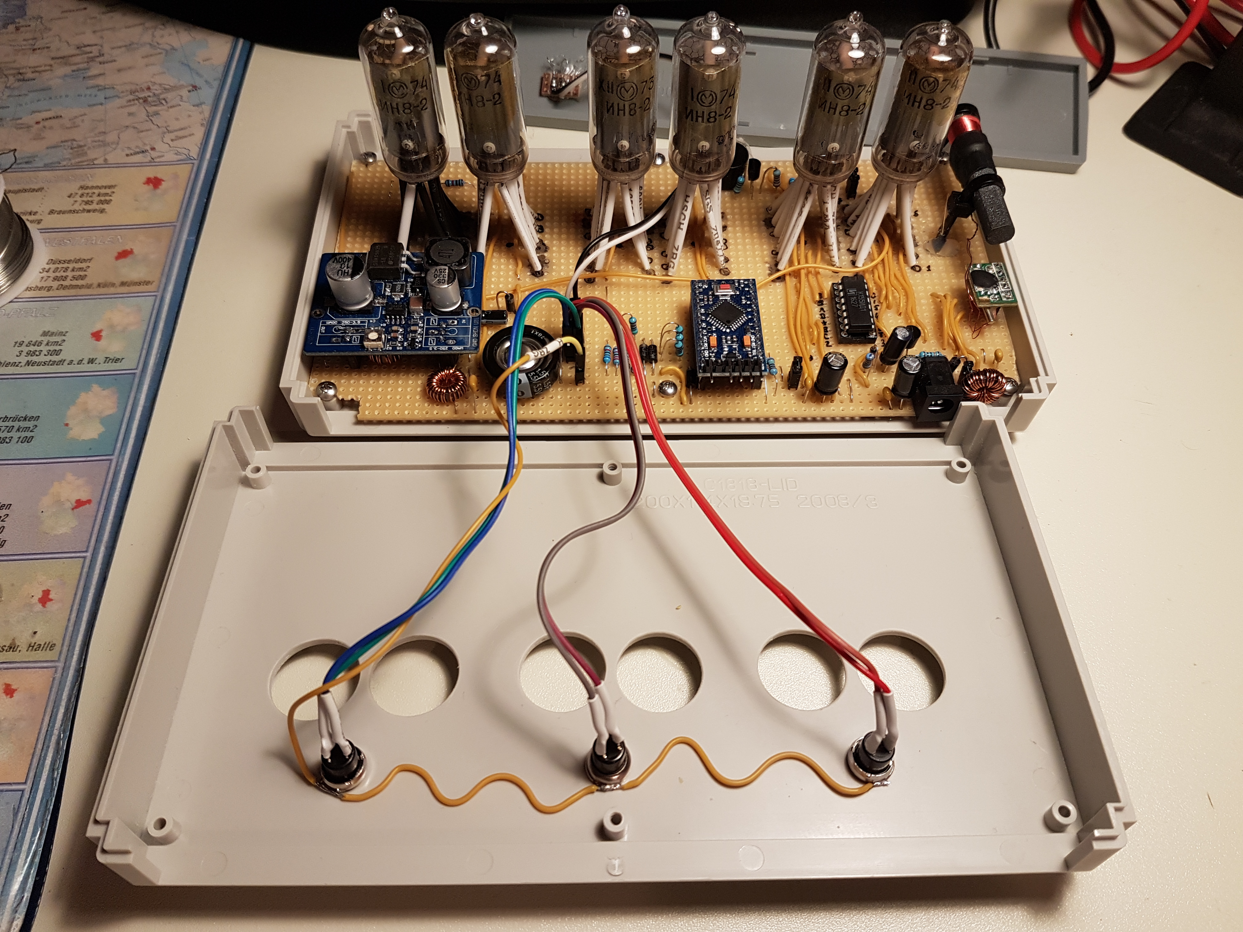
The Nixie Clock consists of the following hardware components as seen on the picture below:
- Nixie tubes
- Arduino Pro Mini board
- DC-DC converter board
- DCF77 reciever board with antenna
- K155ID1 Nixie tube driver IC
- Supercapacitor
- Photoresistor
- Buzzer
- Push-buttons
The clock has been designed around an off-the-shelf enclosure of type “RND 455-00121” with the dimensions of 200 x 121 x 40 mm.
The following picture shows the open enclosure of the Nixie Clock with various components marked in red color.
The circuit has been assembled on a stripboard PCB with most of the components mounted on the top side; except for the optocouplers, voltage regulator and a couple of resistors which are soldered to the bottom side of the PCB. The following picture show the top side of the PCB where the DC-DC converter and Arduino boards have been removed. Note that there is a 220 nF ceramic capacitor hidden under the socket of the K155ID1 IC.
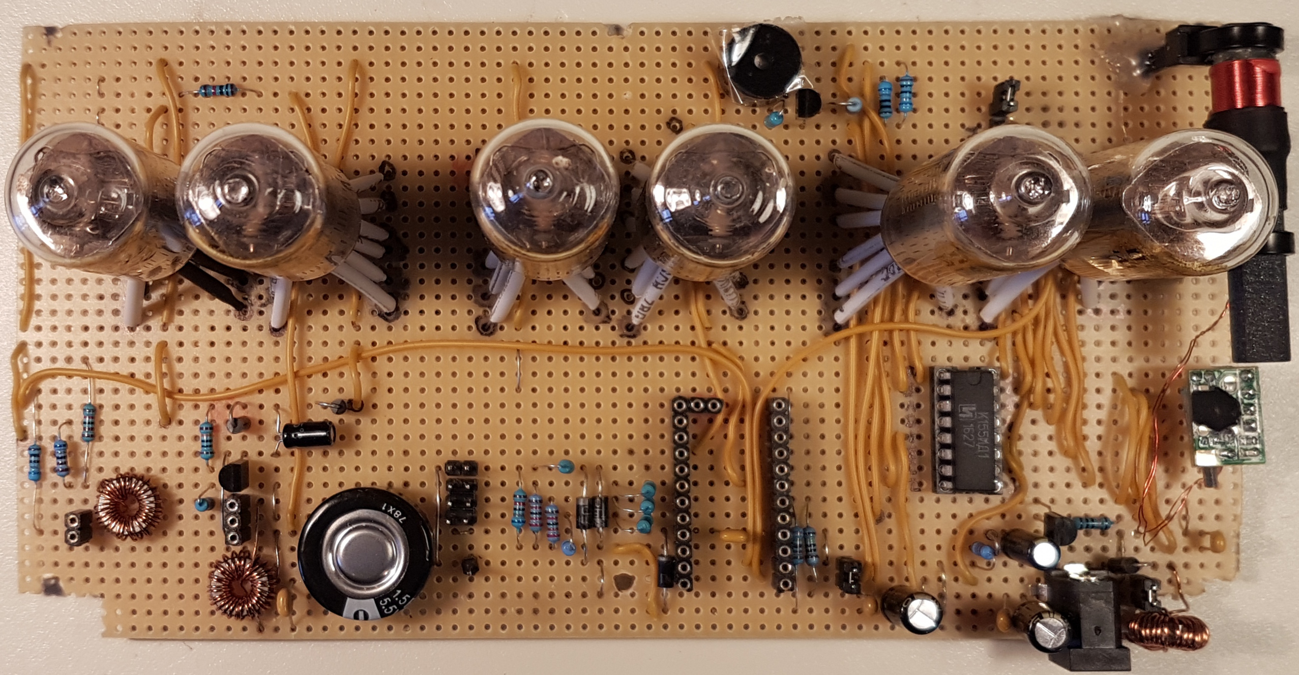
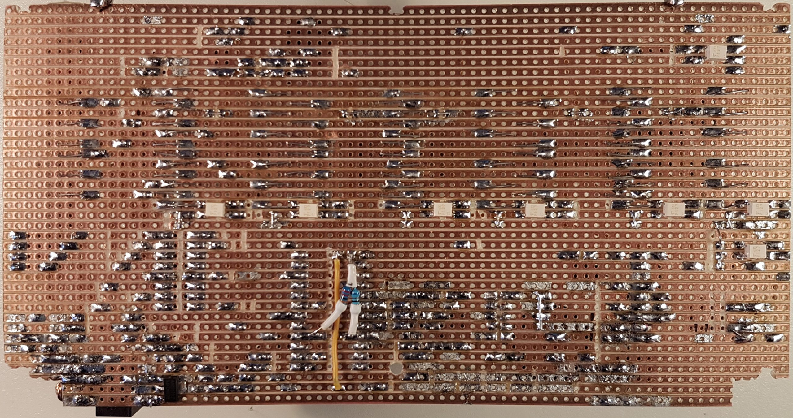
The following picture shows the bottom side of the PCB. Note the placement of the 8 optocouplers (in white) as well as the voltage regulator (bottom-left corner) and 2 resistors. Also note the locations where the copper lanes have been cut.
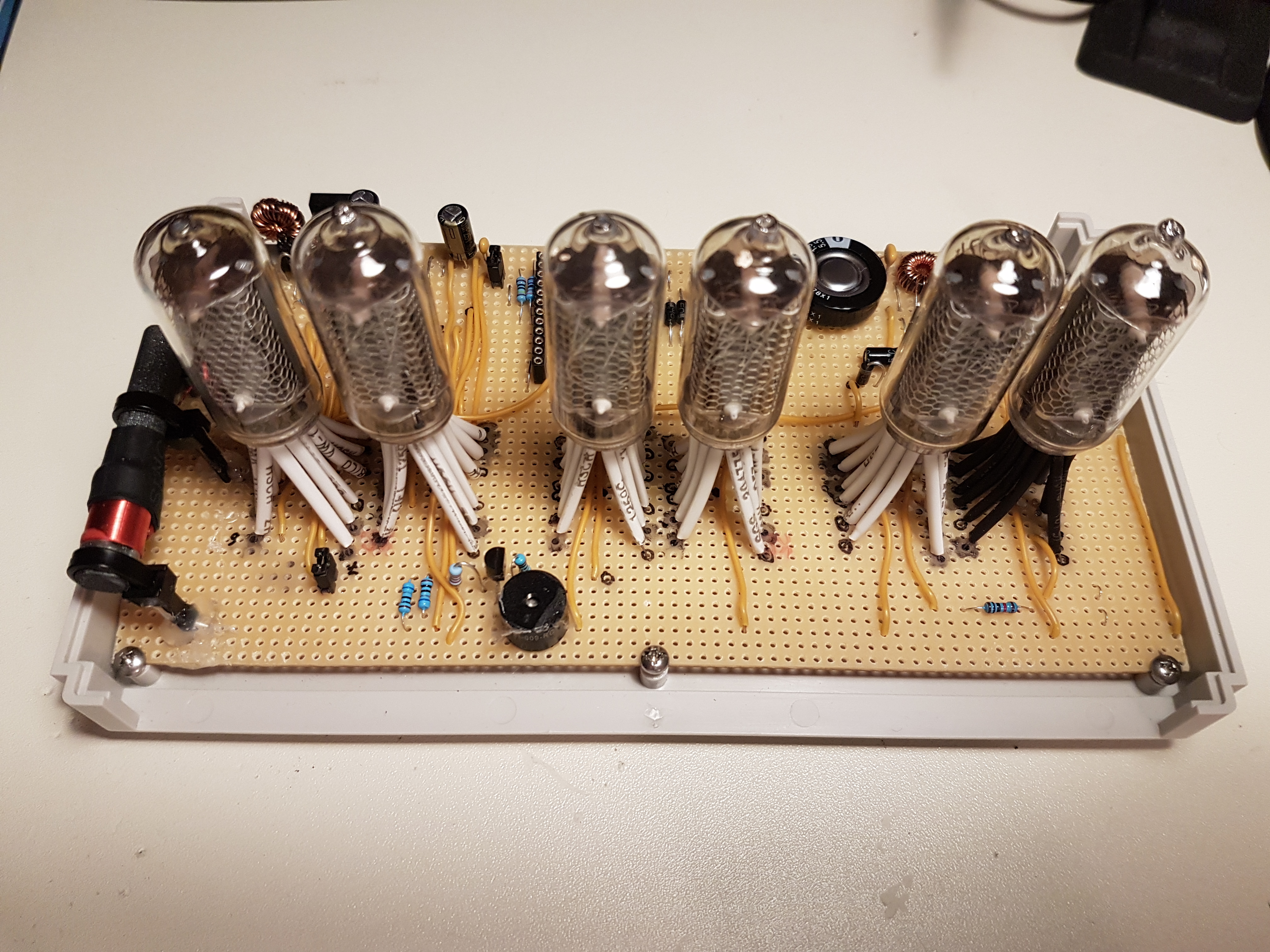
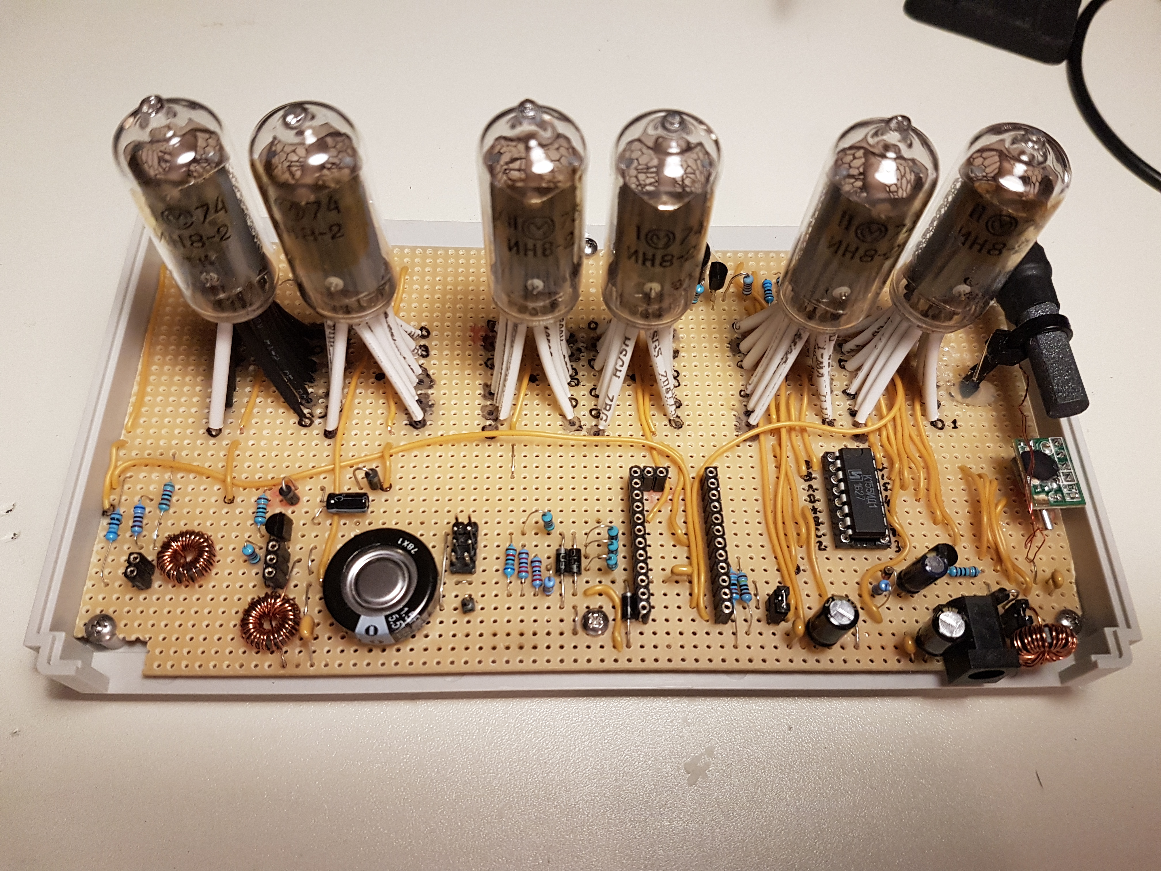
The following picture gallery shows the insides of the Nixie clock from different perspectives.
IN-8-2 Nixie Tube
The following figures show the outline and pinout of the IN-8-2 Nixie tube (source: www.tube-tester.com/sites/nixie/data/I/IN-8-2/in-8-2.htm).
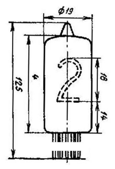
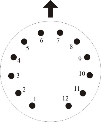
| Pin | Connection |
| 1 | Cathode digit 1 |
| 2 | Cathode digit 2 |
| 3 | Cathode digit 3 |
| 4 | Cathode digit 4 |
| 5 | Cathode digit 5 |
| 6 | Cathode digit 6 |
| 7 | Cathode digit 7 |
| 8 | Cathode decimal point |
| 9 | Cathode digit 8 |
| 10 | Cathode digit 9 |
| 11 | Cathode digit 0 |
| 12 | Anode |
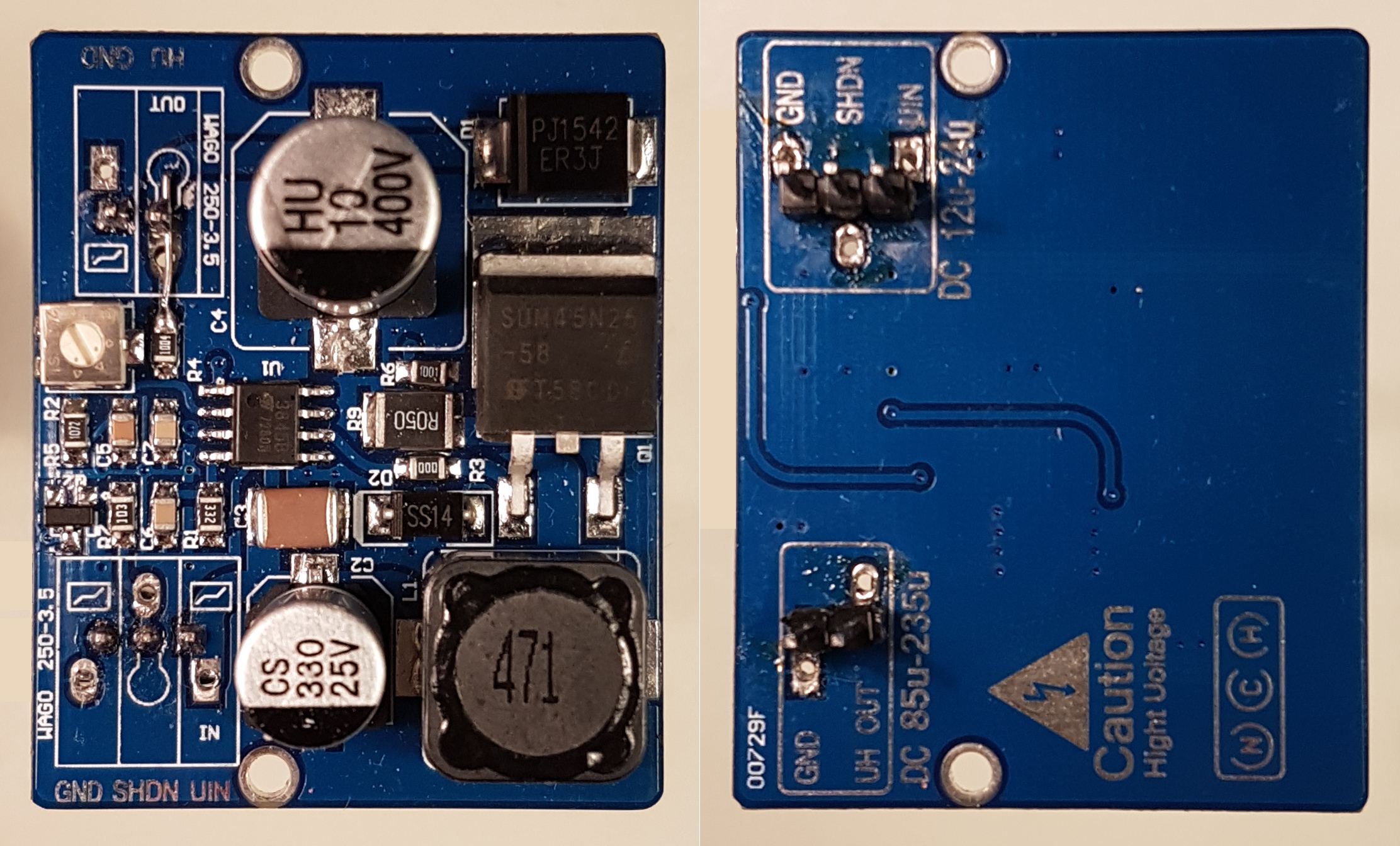
DC-DC Converter
The figure below shows a close-up image of the high-voltage DC-DC converter.
The current device has been running for 5000+ hours and has proven to be very reliable and silent.
Arduino
An Arduino Pro Mini clone with the following modifications has been used in this project:
- in order to reduce power consumption and increase backup power runtime, the onboard power LED and voltage regulator have been desoldered as shown in the following link: https://andreasrohner.at/posts/Electronics/How-to-modify-an-Arduino-Pro-Mini-clone-for-low-power-consumption/
- A custom bootloader with watchdog timer support has been flashed as shown in the following link: https://github.com/microfarad-de/bootloader
Note that there are Arduino Pro Mini boards using a quartz oscillator as well as those using a cheaper a resonator as a CPU clock source. For best clock accuracy over a wider range of ambient temperatures, It recommend to use a quartz oscillator driven Arduino board. (The above pictures show a resonator driven Arduino board, whereas the quartz oscillator has two pins and is much larger in size, as opposed to the barely visible three pin resonator.)
Furthermore, the use of an Arduino Nano (essentially an Arduino Pro Mini with an onboard USB to Serial converter chip) is not recommended as its onboard USB to serial converter would significantly increase the power consumption, thus reduce the runtime on backup power from the super capacitor. It may also interfere withe the buzzer and brightness boost features connected to the RXI and TXO pins that are also being used for serial communication.
Circuit Diagram
The figure below shows the schematic of the Nixie Clock.
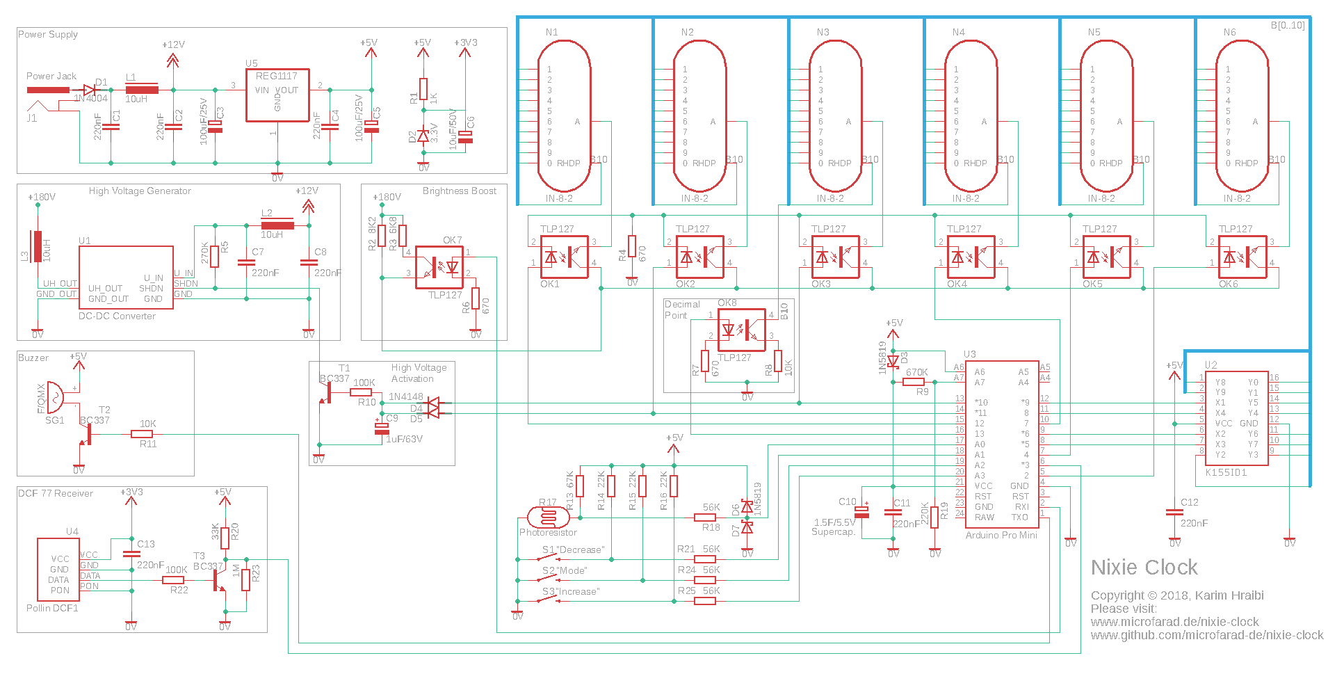
It consists of the following blocks:
- Power supply: generates the voltages required for powering-up the various sub-systems. It uses the AMS1117 (U5) linear regulator for the 5 Volts output and a Zener diode (D2) for the 3.3 Volts.
- High voltage generator (U1): generates the Nixie tube anode voltage of approximately 180 Volts. It uses an off-the-shelf DC-DC converter which was purchased from China on Ebay.
- High voltage activation circuit (T1, D4, D5, C9, R10): as soon as the ATmega microcontroller begins driving the Nixie tube anodes, this circuit detects the periodic pulses on the anodes of tubes N2 and N3 and subsequently enables the high voltage output on the DC-DC converter (U1).
- Brightness boost circuit (R2, R3, R6, OK7): increases the Nixie tube brightness by reducing the value of the anode resistor. This is an exceptional measure for very bright daylight conditions as the brightness is normally controlled via Pulse Width Modulation (PWM).
- DCF77 receiver (U4): contains the “Pollin DCF1” receiver which runs at 3.3 Volts, has a very low power consumption (as it is designed for battery-powered clocks) and has very high output impedence. An NPN transistor (T3) is used for boosting the output signal and making it suitable for the ATmega microcontroller’s input pin.
- Buzzer (SG1): includes an NPN transistor (T2) buffer stage for the buzzer
Further, the schematic contains the following items:
- 6 Nixie tubes (N1 to N6), the optocouplers (OK1 to OK6) for driving the anodes and the decimal point cathode (OK8); and the K155ID1 (U2) cathode driver chip for driving the digit cathodes
- Backup power circuit with a Schottky diode (D3) and a supercapacitor (C10)
- Photoresistor (R17), push-buttons (S1, S2, S3) with their pull-up resistors (R13 to R16) and related input protection circuitry. Notice that due to the shortage of digital pins, the three push-buttons are actually connected to the left-over analog pins. Also note the lack of any debouncing circuitry as button debouncing is being performed in software.
- Three 10 µH (L1, L2, L3) inductors have been placed around the circuit, one standalone and two as part of low-pass networks. These are required for suppressing the high-frequency noise of the DC-DC converter and the 12 Volt switching power supply. Failing to do so would significantly reduce the performance of the DCF77 receiver which is overly sensitive to electrical noise.
Some Electrostatic Discharge (ESD) protection measures have been taken in order to protect the Arduino’s ATmega microcontroller. The push-buttons and the photoresistor are especially prone to for taking ESD due to their location on the outside of the enclosure, the frequent user interaction and their direct connection to with the Arduino’s ADC pins.
In order to prevent ESD damage, the metal bodies of the push-buttons (S1, S2, S3) have been connected to the negative power supply (not shown on the schematic) and current-limiting resistors (R21, R24, R25) have been connected in series with the ADC inputs. This will ensure that any ESD discharge would be diverted to the negative power supply through the bodies of the switches and any residual current is limited by the resistors.
ESD protection of the photoresistor (R17) has been achieved via a current-limiting resistor (R18) in conjunction with a pair of clamping diodes (D6, D7). The clamping diodes deflect the excess voltage due to an ESD event towards the positive and negative power rails, ensuring that the voltage at the analog input pin stays within the range from -VD to VCC + VD. Whereas VD is the junction voltage of the diode (0.3 V for the used Schottky diode) and VCC is the +5 V power supply voltage. The current-limiting resistor protects the clamping diodes from being destroyed by the ESD current pulse.
Notice some minor discrepancies between the below schematic and the pictures shown in the previous section. The schematic shows a couple of additional filtering capacitors (C1, C8) and better-suitable diode types (D4, D5). The schematic does not show any of the jumpers and pin headers present on the PCB.
The above schematic has been implemented using Autodesk Eagle, the related source files can be found under the downloads section below. Please note that the PCB layout has not been yet finalised, however i would be very happy if someone would find the time to contribute.
Downloads
Among others, below you can find GitHub download links for the Arduino firmware source code, user manual and the Eagle schematic source files. All the source code is distributed under the GNU General Public License v3.0.
Please note that the current implementation uses the watchdog timer functionality which requires the customized Arduino bootloader found under the link below. Additionally, ensure that you use Arduino IDE version 1.8.19 to compile the firmware. For more details, please follow the installation instructions found within the README file on GitHub.
Hi Karim, thanks for your answer and availability.
I totally solved the compiling issue without any modification, just using Arduino IDE version 1.8.13
Marco
Hi Marco, glad to hear that.
Hello Karim, sorry to bother again.
When compiling the code in arduino IDE (no modifications in the code) I get this error :
collect2.exe: error: ld returned 1 exit status
exit status 1
what does it means and how I can solve this problem?
Thank You
Marco
Hi Marco,
not totally sure, but this error might be due to missing source files. Did you download the Git submodules by calling `git submodule update –init` within your project root? Otherwise you might download the the full source code zip file “nixie-clock-5.1.1-full.zip” from https://github.com/microfarad-de/nixie-clock/releases and try to build it. Another reason might be the use of the latest Arduino IDE 2.2.1. I’m currently using and older Arduino IDE 1.8.13 and never tried to build with the latest one. Regards, Karim
Hello, thank you very much for this wonderful project.
I am supplying the various components, I have a doubt about the photoresistor. In what range should I purchase it? 5-10Kohm…? 30-50Kohm…? 50-100Kohm?
thank you very much for your support
Hi Marco,
glad to hear that you are implementing the Nixie Clock. I don’t remember the exact value, however given the 67 K series resistor R13, I would go for the 30-50 K or 15-100 K value. Otherwise any of the values you have proposed would do the job, whereas you might want to adjust R13 such that it is roughly equal to the photoresistor’s mid range value. Best regards, Karim
Hi Karim,
I’ve implemented the design on a Nano and it is working in clock mode and stopwatch. However, when I try to navigate through the menus the response from the three pushbutton does not give the expected corresponding digit values, as given in your user manual. I have assumed that using a Nano should be no different that the Pro Mini board you have used for the design. Also, is it possible to monitor the menu states using the serial monitor?
Thanks
Philip
Hi Philip,
both the Pro Mini and the Nano use the ATmega328p and are virtually identical. The only difference is the nano features an on board USB to Serial chip.
For sure you can uncomment #define SERIAL_DEBUG in the .ino file line 70. You can then add some PRINT or PRINTLN statements to the corresponding state machine switch cases. It’s hard to tell what is the root cause of this issue. As with any complex embedded project, bringup issues are totally normal and expected. I’m pretty sure you will be able to resolve the with enough patience and ingenuity.
Regards, Karim
Hi Karim,
Thank you for publishing version 5 that now includes the time zone selection feature. I’m underway with the construction of clock using the Nano V3. In order to ensure that I get the direction of the nixie tubes correct in terms of hours, minutes, and seconds, I’ve checked the code and user guide although I’m still not 100% sure about this. My question is: looking at the clock with hours on the left and seconds on the right, is the order of Nixie anodes 0,1,2,3,4,&5 or 5,4,3,2,1&0 from left to right? Many thanks for all your hard work.
Kind regards
Philip
Hi Philip,
you are welcome! Glad to hear that you have started the implementation and will be happy to see the end result.
Answering your question and having reviewed nixie-clock.ino line 1009, anode 0 corresponds to the rightmost tube that displays the seconds value.
Best Regards, Karim.
Hello Karim,
Your Nixie Clock is a comprehensive design which I’ve decided to build for myself, thank you for all your hard work on this and sharing it with all us Electronics junkies.
I have just one question which is:
For use in the UK. on UTC, using the DCF77 time syncronisation protocol, am I right in thinking I would set my Nixie clock to local time (UTC in my case) and the DCF77 signal will keep that (UK local UTC) in sync and won’t keep trying to advance it to CET/CEST?
Kind regards
Philip
Hi Philip,
thanks for contacting me and glad that you are interested in my Nixie Clock project. The DCF77 signal broadcasts the German time which corresponds to UTC+1 (or UTC+2 when in daylight saving time). The original firmware version is only able to display the German time zone when synced to DCF77. However, I have some good news as I have just implemented multiple time zone support on the latest mainline. The code is ready, however it has not been properly tested nor released yet. It will be part of the upcoming firmware version 5.0.0. For running at UTC, you will have to set the time zone to 0 (setting menu item 1.1) and set the daylight saving to 0 as well (setting menu item 1.2). I hope this helps.
Best Regards, Karim
Hi Karim,
Thanks for replying back, and advice.
I have increased the clock speed of my PIC to 16MHz and the flickering is not so bad anymore, still visible, but not as worse as before.
I then increased the clock speed to the maximum my PIC can handle on an internal OSC to 32MHz, and there was no further improvement to the flickering.
In my tests, I have found that turning one tube ON for longer than 1250 microseconds it gives me a too big flickering.
Lowering the time a tube stays ON will make flickering disappear completely, but will also dim the digit so much that is not worth it.
So, a compromise between the flickering and acceptable dimming of the digit for me is around 1150 microsecs for a tube to be ON.
How did you come up with your 3000 us period for one tube with a maximum ON of 2680 us?
Tests (trial and error), or calculations from a datasheet for your tubes?
Hi Robert,
you are welcome. I came up with the numbers through trial and error tests. 3000us for 6 tubes is equivalent to ~55 Hz flickering frequency, which is about the lowest flicker frequency that is noticeable to human eye. Increasing the on duration beyond 2680 us results in noticeable ghosting, where the a dimmed copy of one tube’s digit would appear in the neighboring tube. If you see some noticeable flickering, then the actual digit period is likely to be higher than 3000 us. Perhaps you should check whether the PIC implementation micros() function is working correctly.
Best regards, Karim
Hi Karim,
Thanks for sharing your project.
I have almost finished a similar project using IN-12A Nixie Tubes, and I have followed your idea of multiplexing the Tubes on a single K155ID chip, and used 4x TLP627-2 Optos.
I have also got a DCF77 receiver, but unfortunately our building is like a metal mesh and I got problems receiving a usable signal. Anyway I put this off until later.
It’s hard for me to read through your firmware, as I do not work with Arduino, but I designed it around PIC18F2520 with a clock of 1MHz
I have started the unit up, and I’ve got problems with the flickering of the Nixie Tubes because of multiplexing.
How did you solve that, or you just left them flickering?
Have you got a video of the clock running so I could see your tubes flickering?
My flickering is so bad I swear it gives you headaches.
How long do you keep one nixie tube ON, and what’s the delay between when you turn one tube OFF until you turn the next tube ON?
Do you think that increasing the clock frequency of the PIC would solve my flickering?
Or is it because my IN-12A tubes are different from yours?
Thanks.
Hi Robert,
thanks for your feedback, glad to hear that you have implemented the project. The IN-12A tubes should work as well, however you have to adjust for the lower anode voltage of 145V (versus 180V-200V for the IN8-2). Also, the IN-12A don’t have a decimal point, which is used for displaying the Alarm and DCF status.
It’s been a while since I last worked with PICs, so it’s hard for me to tell the exact root cause. Nevertheless 1MHz seems to be a bit slow as compared to the 16MHz of the ATmega328P. So the PIC has definitely too little processing power in order to drive the display multiplexing in real time, in conjunction with other tasks such as brightness control and DCF decoding.
As seen in https://github.com/microfarad-de/nixie-clock/blob/master/Nixie.cpp, each digit has 3000 microseconds time slot (DIGIT_PERIOD). In order to avoid ghosting, the maximum allowed on duration is set to 2680 microseconds (MAX_ON_DURATION). Hence, at full brightness, each digit will light-up during 2.68 milliseconds and will bee off during the remaining 0.32 milliseconds. For lower brightness levels, the on/off duty cycle will be reduced accordingly.
All in all, I would strongly recommend using ATmega328P since it is not expensive and there will be no need for porting and debugging the firmware on PIC. I recommend simply taking a 16MHz Arduino Pro Mini board, they are small in size and can be ordered on eBay from China for very little money.
Best Regards, Karim.
PS: please note that I have just fixed a bug in the circuit diagram, where the lines on the Rx and Tx pins have been swapped on the Arduino.
H Karim,
Thank you once again for making such an excellent package available.
I have built the clock and have discovered a minor bug in the .ino which results in the brightness and audio alarm not functioning as they should.
In my .ino version BUZZER_PIN (Rx 0) is given pin number 1 and BRIGHTNESS_PIN (Tx 1) is given pin number 0.
These should read BUZZER_PIN 0 and BRIGHTNESS_PIN 1 as this is the way the Rx and Tx pins are mapped in the ATMEGA 328P pro mini board I am using.
I think this should also solve the problem Luke was having.
Thank you and very man congratulations on the good job you made with this project.
Hi Maurice,
thank you very much for pointing-out the error in the schematic. Yes, I have had some feedback regarding the buzzer not working as it should. I didn’t have the time to investigate the issue, so many thanks for finding the problem. I have uploaded a corrected version circuit diagram, where I have swapped the lines towards the Rx and Tx pins. The pictures of the PCB actually show the correct wiring.
Best Regards, Karim
Hi Karim,
I have also built your excellent circuit and I am trying to couple a more sensitive receiver to it on account of my being over 1500km away and reception is poor.
I have also encountered the same problem as Luke and Rx1 is staying put at GND regardless of alarm status. As suggested by you, I have written a short program to make Rx1 go HIGH and it does so but I have not managed to toggle it between high and low on looping.
The Nixies flash under alarm conditions but no pulse reaches T2 base. The transistor itself is OK and the buzzer can be made to sound if I raise the base voltage. Any suggestions?
My compliments to you on the package. It is the best all round nixie clock for arduino I have seen and it is amazing how you managed to pack so many features into a modest hardware array.
Hi Karim, i would like to say you: “thanks” for sharing your idea.
Hi Pierre, you are welcome!
Hello Karim,
there hex code and pcb drawing, can you send me an e-mail thanks.
I would be very glad if you can send it as pdf to the PCB board
Is it possible to use the hex code continuously?
Hi Ferdi, unfortunately I have no PCB layout available for this design. Please feel free to contribute. Thanks.
Hello
I am just about to take a tentative step into the world of Arduino using an ESP32.
Would the code you have written work in an ESP32?
Best Regards Tom
Hi Tom, sure, I think the code can be ported to ESP32, however with a few modifications. The Nixie clock uses the following ATMega328P hardware blocks: Timer1, Timer2, External pin interrupt and Watchdog timer interrupt. I’m not very familiar with ESP32, however I believe it should have the equivalents of those blocks and more. In conclusion, it won’t work out of the box so you’re going to have to port the code. Feel free to fork and modify the Github project for that purpose. Best Regards, Karim
Hi Karim
I build nixie clock too. Everything work fine, but alarm buzzer doesn’t beep. Arduino led and nixies flash but pin RX(on arduino) has no output. Would you know, what could be wrong? Arduino pin RX is OK. I tested it. I think, it could be something in code…but during compiling no error occurred.
Hi Luke,
Glad to hear that you have built the Nixie clock. Normally RX1 and TX0 act as normal GPIO pins, but they also double as Serial communication pins and are used by the bootloader to download the firmware. In my case, the RX1 pin works as usual, however the buzzer emits some sounds while the firmware is downloading. Could you try to write a sample code that sets RX1 to HIGH and measure the voltage? Did you rule out any issue with the transistor circuit around T2?
Hi. Is there a way to replace the radio receiver with an rtc because this radio is not available where i live?
Hi S.M., I assume that your area is not covered by the DCF77 signal. If so, it is possible use an RTC, however this would require some changes in the firmware implementation. You are going to have to periodically query the RTC and apply the time. There are more details than i could explain in this chat. Nevertheless, please feel free to fork the project and adapt it to your needs. Best Regards, Karim
Hello
I build your watch but the Polini receiver is not available, so I bought one from HKW but with a non-inverted output. Since the DCF library is apparently your development, I don’t know whether the signal can be inverted in the software or whether I should use Transitor?
My programming skills are weak.
By the way, very nice work, thank you.
Best regards Petr
Hi Petr, happy to hear that you have built the Nixie Clock. The non-inverted receiver should work as well. This can be achieved in two different ways:
– If the data pin of the HKW DCF77 receiver provides a high logic level of +5V, then you could omit the transistor T3 and connect the data pin directly to the Arduino. Removing T3 will invert the signal.
– Otherwise, you can modify https://github.com/microfarad-de/nixie-clock/blob/master/nixie-clock.ino line 315 to Dcf.initialize (DCF_PIN, RISING, INPUT);
Best Regards, Karim
Hi Karim,
I agree with you about the 1/6 duty cycle so I have designed a circuit where I use a 50% duty cycle.
I use 3x KM155 and cycle H M S and then h m s at about 60Hz and this is very close to full brightness when I increase the anode current by about 30%
Hi Raymond,
sounds like a good compromise. For my next clock, I’m planning to use a series of TPIC6595 high-voltage shift registers from TI instead of the KM155. These consume way less current and require only 2 Arduino GPIO pins for serial and clock. This design has been implemented by Dave from EEVblog in https://www.youtube.com/watch?v=ggVu_U-CsAk. Also check the schematic in https://github.com/microfarad-de/kicad/tree/master/nixie-clock-v2.
Best Regards,
Karim
At first glance I see a very innovative idea by multiplexing 6 tubes (I braved 2). In order to achieve brightness without flicker, I see that you use 8K2 resistors as current limits on the anodes which suggests a current inrush of about 20mA for about 160mS. Or am I wrong?
My question is: Will this be detrimental to the life span of the tubes?
Kind regards,
Raymond Vaughan
South Africa
Hi Raymond,
thanks a lot for your feedback. 8K2 has been chosen such that the peak current amounts to approximately 4.5 mA (maximum specified current for the IN-8-2). The actual voltage across the resistor is ~180V – V_drop, where V_drop ~140V is the voltage drop across the Nixie tube. Whereas, I presume that you have assumed a resistor voltage of ~170V for your calculation.
The Nixie clock has been running for 2+ years with no signs of degradation. The drawback of such a design is the limited maximum brightness which is 1/6th as compared to a non-multiplexed design. For this reason, I would rather go with a non-multiplexed design for my next project. However, this would require a custom PCB layout because it would be otherwise difficult to fit all of the required components on a prototype board.
Best Regards, Karim
Hello, i tried to build my own nixie clock by this perfect project. So i made the board, put on arduino, dcf receiver, dc-dc converter etc… Then i put on arduino pro mini bootloader and main program. So i switched on it, and it looks like everything works, but after a while i found out that dcf 77 synchronization didn´t work (time didn´t sync). I measured output signal of dcf module and input signal to arduino and everything was ok. Decimal point and arduino led was lit, but nothing happens. So can you help me find out where´s the problem…?
Hi Denis, happy to hear about your successful bring-up. Regarding the DCF77 issue, there might be different root causes, some of them are:
– Noisy power supply
– DCF module provides an inverted signal
– Placement of the DCF77 antenna
When working correctly, the decimal point of the 10s digit (second from right) must blink while DCF sync in progress, whereas the DP goes off when the output of the DCF receiver is high and on when the DCF output is low. The output of the DCF receiver shall go high for 100ms (bit=0) or 200ms (bit=1). I hope this helps.
Best Regards, Karim
Bravo pour cette réalisation , ca donne envie.
Merci!